THE PROF : No exaggeration, but this thread is the best learning experience I have had...
I am checking /replacing stuff systematically, including all the electrolytics.
A funny thing I had noticed in the meantime -- often if a speaker is left connected while powering up, the offset swings to a few volts negative, and comes down a volt or so, but never near say, less than 50 mV. But if you try powering up once again without the speaker connected, then the swing is momentary and corrects itself in a matter of seconds, and all is normal. Very weird indeed...
All the more reason for me to think that the amp could do with a redesign/mod, so that the wacky servo is replaced by a tried and tested LTP that ought to be stable and more predictable.
COGENIAC : I suspect it depends on the speaker. Speaker crossovers have a bunch of reactive components (inductors and capacitors), and they will react differently to DC. The question is, why is there DC at start up?
I'd try disconnecting and shorting the inputs of R647 and R649. This should shut down the output stages. If there is still an offset, then there is something wrong in the output stage. That is usually either a failed transistor, or a failed emitter stabilizing resistor. These are usually low value base resistors (10 ohms) or very low value emitter resistors (0.22 Ohms 2 watt) intended to provide some feedback for thermal drift.
THE PROF : An old single 8 Ohm speaker driver...nothing fancy.
Yes, would try that and isolate the fault to one section ASAP.
I guess I could wire in just one new pair of output devices for testing, instead of all the three pairs?
BTW, I have some doubts here. The 545 being a dc coupled amp, won't the input signals be present even if C611 is removed? I have seen a range of cap values in many similar circuits, and never once thought that it was a signal coupling cap. The Vbe thermal compensation transistor (Q618) is bolted to the main heatsink, and I had though this cap was meant to "smooth out" any sudden variations in bias.
COGENIAC : The input signal will leak through the bias circuitry, but the positive and negative signal levels would be significantly different. The 4.7 uF cap is certainly a coupling cap.
Biases set the operating point for the transistor, and they should not waver, so there would be no reason to "smooth out" variations.
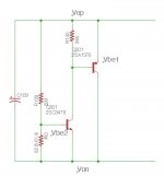
Yeah, I find that interesting. So they are using the Vbe change over temp to adjust the bias. What's odd here is that they only have a partial circuit for this. If you look at posts 381 and 382, I have the bias temp control for the 565. Here the Vbe of the transistors is used to drive the operating points down as the temp rises. Top is the positive bank input signal line, and Von is the negative bank input line. Q201 is on the positive bank heatsink, and Q301 is on the negative bank heatsink. The two transistor circuits are intertwined in an interesting way. Here is the schematic again, and I'll repeat the explanation with some added observations.
From this circuit, you can see that as the temperature of the junction of Q301 goes up, Vbe2 will go down, thereby increasing the current drawn through R139. The current through Ro will actually decrease, because the voltage across Ro (Vbe2) is lower, which means the base current of Q301 will increase. This will cause the collector current of Q301 yo increase, thereby increasing the current through Q201. This increased current will cause Vce of Q201 do decrease, which means Von and Vop will be pulled toward a virtual ground (i.e. each will be pulled toward the other). This lower offset will then reduce the current through the output Darlingtons, thereby lowering the temperature.
Similarly, if Vbe goes down (as the positive heatsink temp rises), the current through R140 will go own (because the drop across it is lower). However, the current the collector of Q301 is fixed by the other elements, and if they have not changed, this reduction in R140 current will increase the base current of Q201 and further pull the inputs lower.
As was noted by Phoodpants, in the 585 amp, they kept one of these transistors on the board, and only one was on a heatsink. I suspect they found that it didn't matter as long as ONE of them was on a heatsink, that temp will lower the bias in BOTH the positive and negative output banks. Thereby keeping them balanced and also reducing the overall current level.
This circuit is also supposedly used, however, to steer the bias between the positive and negative banks.
The resistor Ro in the diagram is actually a series combination of a fixed resisted and a pot, pretty much like VR601 and R643 in the 545 diagram. In this circuit, if Ro is decreased, then the current in the base of Q301 will decrease (because the current in Ro will increase). That decrease will reduce the collector current in Q301, which will cause base current in Q201 to decrease (because the Vbe of Q201 is fixed, and that means the portion of the Q301 collector current flowing through R140 must be fixed, and this means the reduction in Q201 current must be found by reducing the base current in Q201). This will cause Vop and Von to move away from one another (Vop becoming more positive and Von more negative). Moving the pot in the other direction will have the opposite effect.
I find this interesting, since I had always thought the bias pot was used to steer the offset one way or the other, but it really looks like it just runs the biases up and down together, essentially controlling how much class-A conduction the amp has a zero input. I note that this is counter to what the manual says, so I may not be understanding the operation the pot properly.
Biases set the operating point for the transistor, and they should not waver, so there would be no reason to "smooth out" variations.
Yeah, I find that interesting. So they are using the Vbe change over temp to adjust the bias. What's odd here is that they only have a partial circuit for this. If you look at posts 381 and 382, I have the bias temp control for the 565. Here the Vbe of the transistors is used to drive the operating points down as the temp rises. Top is the positive bank input signal line, and Von is the negative bank input line. Q201 is on the positive bank heatsink, and Q301 is on the negative bank heatsink. The two transistor circuits are intertwined in an interesting way. Here is the schematic again, and I'll repeat the explanation with some added observations.
From this circuit, you can see that as the temperature of the junction of Q301 goes up, Vbe2 will go down, thereby increasing the current drawn through R139. The current through Ro will actually decrease, because the voltage across Ro (Vbe2) is lower, which means the base current of Q301 will increase. This will cause the collector current of Q301 yo increase, thereby increasing the current through Q201. This increased current will cause Vce of Q201 do decrease, which means Von and Vop will be pulled toward a virtual ground (i.e. each will be pulled toward the other). This lower offset will then reduce the current through the output Darlingtons, thereby lowering the temperature.
Similarly, if Vbe goes down (as the positive heatsink temp rises), the current through R140 will go own (because the drop across it is lower). However, the current the collector of Q301 is fixed by the other elements, and if they have not changed, this reduction in R140 current will increase the base current of Q201 and further pull the inputs lower.
As was noted by Phoodpants, in the 585 amp, they kept one of these transistors on the board, and only one was on a heatsink. I suspect they found that it didn't matter as long as ONE of them was on a heatsink, that temp will lower the bias in BOTH the positive and negative output banks. Thereby keeping them balanced and also reducing the overall current level.
This circuit is also supposedly used, however, to steer the bias between the positive and negative banks.
The resistor Ro in the diagram is actually a series combination of a fixed resisted and a pot, pretty much like VR601 and R643 in the 545 diagram. In this circuit, if Ro is decreased, then the current in the base of Q301 will decrease (because the current in Ro will increase). That decrease will reduce the collector current in Q301, which will cause base current in Q201 to decrease (because the Vbe of Q201 is fixed, and that means the portion of the Q301 collector current flowing through R140 must be fixed, and this means the reduction in Q201 current must be found by reducing the base current in Q201). This will cause Vop and Von to move away from one another (Vop becoming more positive and Von more negative). Moving the pot in the other direction will have the opposite effect.
I find this interesting, since I had always thought the bias pot was used to steer the offset one way or the other, but it really looks like it just runs the biases up and down together, essentially controlling how much class-A conduction the amp has a zero input. I note that this is counter to what the manual says, so I may not be understanding the operation the pot properly.
Attachments
COGENIAC : Some additional thoughts on the bias control in the 545.
Based on the voltage drops across R636, and the series combination of R640 and R642, the current in the Q616 current source is about 6.7 mA.
The drop across R646 (681 ohms) is .7 volts, so the current through R646 is .7/681=1.02 mA. Since the current in VR601 and R644 is the sum of the base current in Q168 and the 1.02 mA flowing in R646, we can determine the nominal value of VR601 is about 827 Ohms. (odd that it is much bigger than 2x this. Might have just been what was available).
This means that in this nominal situation theQ618 transistor is passing about 5.7 mA.
If we decrease the resistance of VR601, then, in order to keep the 1.02 mA current flowing, the voltage at the collector of Q614 must increase. Since the current has not changed, the voltage on the current source is unchanged, so the voltage at the input of Q622 will not change. This means decreasing the resistance of VR601 will bias the positive side output bank more heavily.
If we increase the resistance of VR601, then the voltage at the collector of Q614 will need to go down to maintain the current flow through R646. So that will then cause the positive side output to be biased less heavily.
So far, we have assumed that the current in the base of Q618 is negligible. If we relax that constraint, I think what happens is that a reduction in the resistance of VR601 will slightly increase the base current of Q6128, thereby increasing the share of current that Q618 conducts. However, since the current source is fixed, it will respond by raising (less negative) the voltage at the collector of Q616. Thus, when VR601 is reduced, the positive output stage bias will increase, and the negative side will decrease. Similarly, if we increase VR601, the base current of Q618 will decrease, thereby reducing the collector current in Q618, and to maintain the proper constant current, the current source will reduce the voltage (more negative) at the collector of Q616. So decreasing the resistance of VR601 will bias the negative output side more heavily and reduce the bias on the positive side.
As the temperature of Q618 increases, its Vbe will decrease, reducing the current flow in R646, and thereby turning on Q618 more heavily. Since this transistor directly connects the two bias points, the reduced effective resistance between them will cause the current source to increase the voltage (less negative) at the output, and since VCE of Q616 will decrease, the current source will drag the positive side down. thus as Q618 heats up, the bias on both sides will go down.
This is really very compact and clever approach to simultaneous bias balance and thermal control. And the trick to it is the use fo the current source.
Attachments
THE PROF : I checked/measured most of the components of both the modules, put in a pair of fairly matched C1845s for the LTP, replaced all the diodes, the trimpots, the electrolytics etc, with generous cleaning and re-soldering, and the R channel came up all right, with less than 9 mV of offset. Same routine for the L channel, but then there was that "hunting" before the output offset settled around 10-14 mV-- with only ONE pair of output devices wired in.
In both cases, with the DC error amp removed (I had wired in a socket), the offset swung to -6V approx, unaffected by R620 (replaced by a trimpot) being tweaked. Once or twice the earlier problem of the offset being "stuck" at a few volts negative if the speaker was left connected came up. Without the speaker, the output "hunted" a bit and settled near zero. Typical erratic behaviour from early on.
It looks like something has given me the slip, though I was careful in checking both the Left and Right channel modules and doing identical 'restoration'. Quite likely it is something simple right before my eyes, though I can't see it now.
COGENIAC : Seems weird. Can you measure the voltages on the input sides of R648 and R650? These should be about 1.7 volts, and -1.7 volts respectively. If these are stable at about this voltages while the output is gyrating around, then the issue is in the output section (which is my suspicion). If this is the case, then measure the voltages in the output stages.
I suspect you have a bad transistor or a bad resistor in the section. A bad positive side transistor might have a normal beta until it warms up, and thus the positive side would start up OK, but then fade and become unbalanced after some time, and not be balanced against the negative side.
THE PROF : I will do detailed voltage measurements ASAP and post.
I had checked all the resistors. Now that you mention it, I too have a feeling that it must be one of the transistors going wonky after warming up. Funny thing is, it is reasonable with one pair of output devices, but goes bonkers more easily with all the three wired up. Q624/626 are new, but Q612 to 622 are old ones, though tested. It surely is an erratic thing that comes up after switch on and slight warming up of the amp.
COGENIAC : Seems like maybe it is not the actual output devices, but is the pre-driver. Q619 or Q621. If that device beta, and or Vbe change substantially with temperature, then as the amp warms up, the positive output will be driven less hard, and the output voltage could drift negative.
But check the voltages on the input resistors R647 and R649 (right channel) and R648 and R650 (left channel) first.
Seems like too much offset to attribute to VBE drift, since the output stage has unity voltage gain.
Also, have you checked the power supply rails? Are they stable when it is doing this offset thing?
THE PROF : Faulty output devices could be ruled out as I have put in a new pair.
Rails are stable and equal.
COGENIAC : Yeah, just work your way back from the R648/R650 input resistors. As I said, those should be +/- 1.7 volts. If not, then the issue is upstream.
As I noted in some earlier posts. the 545 is not fully balanced from start to finish. It is unbalanced class A at the start. Class A meaning two things: a) the transistors are conducting throughout the signal cycle, and b) the "zero" signal crossing point is not at zero, but is elevated to some fraction of the rail voltage. You can see this in the left channel schematic, where at zero input signal, the collector of Q602 (the input transistor of the LTP) and the base of Q614 (the middle stage driver transistor) are at 55.2 volts.
The 565 is similar, except the entire negative side has its own circuit, so in that amp the positive and negative sides are completely separate until they meet at the output stage emitters.
The positive/negative side balance in the 545 is formed by the current source Q616 and the bias adjustment circuit made up of the pot VR602, R6664, and R646. This creates two signal paths, one offset +1.7 volts, and the other offset -1.7 volts. And those drive the positive and negative side stages.
Another possibility is that one of the two current sources is drifting. There are two of them. One formed by Q610 and the two diodes (D602 and D604). That current source generates about 4 mA, which flows through the heat sink thermostat, and powers the diodes D605 and D606. Together with Q616 these form the current source that is responsible for creating the balanced split of the signal on side centered at 1.7 volts, and the other at -1.7 volts.
If that current source drifts, then it would definitely cause an offset. So, another experiment would be to measure the voltage across those two diodes from startup. if that voltage changes as the output offset grows, then it is either the diodes, or the Q616 transistor, or the Q610 current source that is causing the drift.
ANATECH : The outputs should always be replaced as a set. Period. Matching them always helps improve performance. In the old days long before the internet, some service manuals pointed this out. Marantz was probably the most knowledgeable in this regard, and not only with the output stage.
One thing to consider in a failed output stage is that all the devices were stressed beyond their ratings. The failed devices are only the ones that went first. If an NPN went, then the opposite polarity had to handle additional stress since the NPN supply was connected directly to the speaker output in most designs.
Placing the transistors beyond their maximum ratings (and probably even below that) will change their characteristics. That means damage has occurred even though outright failure had not occurred yet. In addition to all that, the diff pair(s) have now lost control of the DC offset and often they will be reversed biased on one side, causing E-B reverse breakdown. This very often will change that part and may also make it noisy or intermittent possibly. For sure it does make the pair unmatched. This isn't someone imagining what could happen, I have directly observed this from the time I was a young technician (40 some years ago) and actually corrected these conditions. I always tested pulled parts for beta and leakage in both modes. Learned lot doing that. I used a Heathkit IT-18 in the early days, and I still use it to check for leakage to this day.
DC offset issues like you are seeing are always (except in rare really weird cases) a problem in the voltage amplifier stage. Typically Diff pair(s) or Vas transistors, but could be in related circuits or components. So focus your attention in that area.
THE PROF : Replaced Q614 and Q616, both Betas around 400 plus. No offset (with one pair of new output devices, servo IC in, and switch on without speakers connected), plays audio.
My rails are just a bit low because of the 'series bulb' protection, and Q614 collector is at 1.5 V plus, while Q616 is only at -0.7V.
A speaker plugged in before switching on mostly results in an output swing to -5 to -6 V. Just disconnect the speaker for a moment, and the offset is reduced to normal. Servo amp doing its job, it looks like..?
COGENIAC : Does the voltage swing only occur with the speaker connected? Or does it swing to -6 volts and then go back to near zero? If you turn it on with no speaker connected, then does the output stay near zero when you turn it on? (that is does it not swing too -6 volts at all?). After it has settled down, does it randomly swing negative again, or is the issue just at start up?
The offsets you measured are a bit puzzling. if the collector of Q614 (positive side of the amp) is higher than the collector of Q616 (the negative side of the amp) then I would expect that the offset would be positive, not negative. Double check the polarity of your volt meter.
The offsets at the collectors of Q614 and Q616 should be the same and opposite polarity. If the output offset is only at startup, then I suspect you are seeing the offset from those mismatched collector voltages and then the servo time constant catches up to the output and corrects it (that is, the servo may have a slow time constant - since you do not want it to react to the audio signal, and it may take a few seconds to react.).
Also, does Q618, or the heat sink itself, heat up?
Try this:
- If the pot changes as expected (maximum resistance of about 2 K Ohms and a minimum resistance of about zero), then remove and test Q618.
Q618 is supposed to change the bias on both sides up and down with temperature. However, if it is open, then this would probably mess up the balance. More likely though is that the pot is open/shorted or does not change its resistance properly.
If changing the trim pot changes the collector voltages (Q614/616) then adjust the pot until the voltages are equal and opposite polarity.
The other thing you could try is to disconnect Q618 entirely. In this case you will have a resistance of between 2500 ohms and 4700 ohms between the collectors of Q614 and Q616, and adjusting the trim pot should cause the voltages at the collectors to change in opposing directions.
-->What I am looking for here is if the bias offset control is working correctly (or is working at all).
Now, if the amp is stable and has zero offset without the servo, attach your volt meter to the speaker terminals, and connect a speaker to it, while it is powered on. if the voltage changes significantly, immediately disconnect the speaker.
-->What I am looking for here is if the presence of the speaker is causing the offset.
If connecting the speaker causes the otherwise zero offset to swing in one direction or another, then the issue is related to current flow (there is little current flow with no speaker connected.) You said that the output transistors were replaced with known good devices. Did that include Q620 and Q622?
The voltage gain of the output sections (ie. Q620 and the output devices Q624-Q636) is unity. If either Q620 or Q650 has a base emitter short, then when the speaker is connected, the current flow through the good one will have one value, and the current flow through the other will have a different value. This will bias the output sides differently and produce an overall offset at the output, but ONLY when there is current flowing in the output stage (ie. when the speaker is connected).
BTW, I recommend getting a big 8 ohm resistor for testing the amp. I have a 350 watt resistor I use for this. It can take full rail current for a brief time, so I can test the amp without killing a speaker.
The offsets you measured are a bit puzzling. if the collector of Q614 (positive side of the amp) is higher than the collector of Q616 (the negative side of the amp) then I would expect that the offset would be positive, not negative. Double check the polarity of your volt meter.
The offsets at the collectors of Q614 and Q616 should be the same and opposite polarity. If the output offset is only at startup, then I suspect you are seeing the offset from those mismatched collector voltages and then the servo time constant catches up to the output and corrects it (that is, the servo may have a slow time constant - since you do not want it to react to the audio signal, and it may take a few seconds to react.).
Also, does Q618, or the heat sink itself, heat up?
Try this:
- Remove the servo op amp.
- Start up the amp
- Measure the output offset, and the voltages at the collectors of Q614 and 616. Record these.
- If the collector voltages are not equal and opposite, then adjust VR602 (the trim pot).
- If rotating the pot does not make any difference, then test the pot.
- If the pot changes as expected (maximum resistance of about 2 K Ohms and a minimum resistance of about zero), then remove and test Q618.
Q618 is supposed to change the bias on both sides up and down with temperature. However, if it is open, then this would probably mess up the balance. More likely though is that the pot is open/shorted or does not change its resistance properly.
If changing the trim pot changes the collector voltages (Q614/616) then adjust the pot until the voltages are equal and opposite polarity.
The other thing you could try is to disconnect Q618 entirely. In this case you will have a resistance of between 2500 ohms and 4700 ohms between the collectors of Q614 and Q616, and adjusting the trim pot should cause the voltages at the collectors to change in opposing directions.
-->What I am looking for here is if the bias offset control is working correctly (or is working at all).
Now, if the amp is stable and has zero offset without the servo, attach your volt meter to the speaker terminals, and connect a speaker to it, while it is powered on. if the voltage changes significantly, immediately disconnect the speaker.
-->What I am looking for here is if the presence of the speaker is causing the offset.
If connecting the speaker causes the otherwise zero offset to swing in one direction or another, then the issue is related to current flow (there is little current flow with no speaker connected.) You said that the output transistors were replaced with known good devices. Did that include Q620 and Q622?
The voltage gain of the output sections (ie. Q620 and the output devices Q624-Q636) is unity. If either Q620 or Q650 has a base emitter short, then when the speaker is connected, the current flow through the good one will have one value, and the current flow through the other will have a different value. This will bias the output sides differently and produce an overall offset at the output, but ONLY when there is current flowing in the output stage (ie. when the speaker is connected).
BTW, I recommend getting a big 8 ohm resistor for testing the amp. I have a 350 watt resistor I use for this. It can take full rail current for a brief time, so I can test the amp without killing a speaker.
COGENIAC : The two things I am suspicious of are these:
1) The bias adjusting resistor VR602 (trim pot) should allow you to control the bias voltages on Q6714 and Q616. If it doesn't then that needs to be remedied.
2) It sounds as if the output offset depends on a load (e.g. speaker) being connected to the output. If this is the case, then drawing current through the amp output is creating the offset, which means the output is not controlling the current through the load. That is probably a problem with Q620 or Q622.
As I noted above the voltage gain from Q620/Q622 through the rest of the amp is unity (no gain), so that section should not be amplifying any offset. Yet you are seeing 6 volts offset with a speaker attached, and the voltage offset at the input tot he unit gain stage (614/616) is only 0.7 volts. SO SOMETHING ELSE is causing that offset.
However, if one of Q622 or Q624 are faulty, that may only show up when current is being drawn through them. In addition, if one of those is faulty, then that fault could distort the bias control circuit, and the combination of low current gain on one side (e.g. the positive side) and some bias offset would cause the output to swing negative when the speaker was attached.
For example, if Q622 has an open collector-emitter junction, then the drive current for the output transistors will be about 100X lower on the positive side. You will still see unity gain but the positive side will be current starved. So when a load is applied any offset in the amplifier gain stage bias (Q614/616) will be amplified by the difference in current flow from the two sides of the output.
The bias offset control (VR602) seems to be working correctly. It is supposed to adjust the offset between the positive and negative sides of the output circuit, and it appears to be doing just that.
Until you get the output working under load, the voltage across the emitter resistor test point is not going to tell you much.
The voltages at the collectors of Q614 and Q616 are a bit low, but that may be a result of whatever is causing the speaker induced offset. If you wanted to adjust that, you could use a pot at R636. This should change the bias on BOTH Q614 and Q616 equally. (the "control for setting the quiescent bias current" you mention above).
The more concerning thing is the speaker induced offset. Clearly that is not correct. Since you are able to get audio output with no load, and since you can adjust Q614/Q616 bias to get equal collector voltages, the issue is in the output stage.
With no load (i.e. speaker disconnected), the output transistors are not actually passing any significant current. As I noted in my last post the entire output section is an "emitter follower" circuit, and that has no VOLTAGE GAIN (or as we say, "unity" voltage gain - a voltage gain of one). So, whatever signal voltage is applied TO the output will be reflected as the voltage AT the output. Instead, the output stage has massive CURRENT GAIN. This is necessary to allow the amp to swing the voltage at the input of the output stage (the collectors of Q614 and Q616) across a low resistance load like an 8 Ohm speaker.
Consider this: If the voltage swing across the speaker load at full volume is, say 49 volts (which corresponds to 150 watts RMS at the output), then the output stage needs to supply 6 Amps of current to an 8 ohm load. Obviously Q614 and Q616 are unable to supply that current, so the output stage simply uses that voltage signal, and adds the ability to drive that voltage across the lower speaker load (i.e. supplying current gain but not voltage gain).
Now, here comes the tricky part. Since the voltage gain of the output is unity, it may be possible for either Q620 or Q624 to be inoperative, and STILL show the full voltage across the output WHEN THERE IS NO LOAD (speaker disconnected). this is because in that situation there is nearly no current flowing in the output stage. If the emitter-collector junction of Q620 is open, but the base-emitter junction is OK (or shorted), that transistor will pass the voltage at the base, to the emitter (which will be about the same as the signal on the collector of Q614). However, since the open emitter-collector junction means that that transistor cannot pass any current, the only current that will flow into the base of the output transistors (Q624-Q636) will be the BASE current of Q620.
The output stage is what is known as a "Darlington" circuit. A Darlington circuit has the emitter of one transistor connected to the base of the next transistor. A transistor is inherently a current gain device, and the current gain is known as "Beta". Beta is the ratio of collector-emitter current to base-emitter current. In a Darlington circuit, the base-emitter current (Ibe) of the first transistor causes a collector emitter current (Ice) of Ice=Beta(Ibe), so the emitter current is Ie=(Ice+Ibe)=Ibe(Beta+1), If Beta is large , say over 100, the +1 hardly matters, so we can write this as Ie=Ibe(Beta) - but remember this, because it is going to come back later.
Note that in the Darlington, the emitter current of Q620, flows directly into the base of Q624. Since the Q624 circuit is set up the same as the Q620 circuit, the emitter current of Q624 is Ie=(Ie'Beta')Beta (where Ie' and Beta' are the current and beta associated with Q620, from the above discussion. Looking at the next stage, the emitter of Q624 feeds into the bases of Q626, Q632, and Q636. These devices are connected in parallel, but the same analysis applies to each of them. The emitter current of Q624 splits into three branches, one for each device, and goes directly into the bases of each of these devices. This means that the emitter current of these devices (Q626, Q632, and Q636) is Ie=(Ie'Beta')Beta''Beta, where Ibe' is the base current of Q620, Beta' is the beta of Q620, Beta'' is the beta of Q624, and Beta is the beta of the output device Q626. Assuming that the Betas of these devices are all about the same, this means that the current gain of this triple Darlington is Beta^3, or Beta cubed!. If the Beta of each device is 100, then the beta of the triple Darlington is one million! So, a 6uA (micro amp) base current at Q620 will produce 6 Amps at the emitters of the output transistors (roughly speaking.. it is a bit more complicated given the three parallel output transistors, but you get the point).
However, let's examine what would happen if the collector emitter junction of either Q620, or Q624 were open, but the emitter base junctions were OK or were shorted. In this case the VOLTAGE at the base would get passed on to the emitter, but the current in the emitter leg would just be the base current. Remember the Beta+1 term we ignored above? Let's write out the actual current equation.
The base current of Q620 is Ibe', so the emitter current is Ibe'(Beta+1), and the overall emitter current at the output of the amplifier is Ie''=Ibe'(Beta+1)(Beta+1)(Beta+1). This is just the Beta cubed relation above, but with the base current terms included.
If either of the collector-emitter junctions of Q620 or Q624 are open, then this changes to
Ie''=Ibe'(Beta+1)(Beta+1)(1), because one of the transistors has no collector current and thus has no beta value.
If one side of the output has a current gain of (Beta+1)(Beta+1)(1), and the other has a current gain of Ibe'(Beta+1)(Beta+1)(Beta+1) then WHEN A LOAD IS APPLIED, one side will be driven with MUCH more (100x) current than the other. HOWEVER, WHEN NO LOAD IS APPLIED to the output, the difference is beta between the two sides will not matter (or at least won't matter very much).
So, I suspect that the collector-emitter junction of either Q620 or Q624 is open, and the base-emitter junctions are either shorted or are OK. When your speaker is disconnected, the current flow is very low, and the difference in current gain has little effect on the output. It probably has SOME effect, but that is adjusted out by the bias control pot (VR602). When the load (speaker) is connected, the current draw increases, and presumably the imbalance between the two sides causes the output to be drawn down by the properly operating negative bank of the output circuit.
Because of the circuit topology, determining which transistor is bad may be a little bit difficult. One thing you MIGHT try is looking at the voltages on both sides of R660 and R662. These should be equal and opposite under load (with the speaker/load attached). If the voltages on either side of of R660 are not the same, the I would suspect the culprit is Q620. If those are OK, but the voltages on either side of R662 are unbalanced, then the problem is Q624.
THE PROF : That sure was a great theory class by 'Prof' Scott, and it served to clarify things even for those like me who are total strangers to the rigours of an engineering classroom! But I admit it took a few reads for my brain to cool down and come out of the knots of theory ...
It is apparent that the component replacements beginning with the LTP pair and up to Q614/Q616 and the associated parts have cured a lot of problems. After adjusting VR602, the voltages are symmetrical there (though a bit low as the rails too are low on account of the series bulb protection).
Without a speaker/load, the amp starts up, the output goes to a max of nearly -6V and settles to 'zero' within about 2 seconds plus. Then the voltages at the two ends of R660 and R662 too are symmetrical.
But what happens when the speaker/load is connected (while the amp is on, with offset at zero), then both the negative voltages (Q622/Q626 end) fall to about half the positive value. But the output offset stays at very near zero without change.
Both Q620 and Q622 measure okay on a transistor/FET tester, though with widely differing Betas. But I don't have ready replacements to try, as their voltage ratings are pretty high; I am getting a substitute pair in a couple of days.
Q624/Q626 as well as the output pair (one pair only wired up) are new devices.
Hope this should lead you to smoking out the "guilty party".
Awaiting your guidance there.
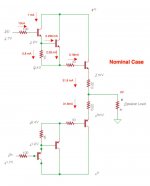
I am still confused about labelling of the bias setting pot. It is supposed to set the class AB operating point, and as such should not affect the output offset. But here Adcom advises setting the bias so that it produces about 7mV across the output device emitter resistor. (I have attached the excerpt from the service manual.) But when that control affects the symmetry of the voltages at the collectors of Q614 and Q616, what does one aim for as the best option--symmetry of the +/- voltages, or the recommended bias current indicated by the 7mV level ??
It is apparent that the component replacements beginning with the LTP pair and up to Q614/Q616 and the associated parts have cured a lot of problems. After adjusting VR602, the voltages are symmetrical there (though a bit low as the rails too are low on account of the series bulb protection).
Without a speaker/load, the amp starts up, the output goes to a max of nearly -6V and settles to 'zero' within about 2 seconds plus. Then the voltages at the two ends of R660 and R662 too are symmetrical.
But what happens when the speaker/load is connected (while the amp is on, with offset at zero), then both the negative voltages (Q622/Q626 end) fall to about half the positive value. But the output offset stays at very near zero without change.
Both Q620 and Q622 measure okay on a transistor/FET tester, though with widely differing Betas. But I don't have ready replacements to try, as their voltage ratings are pretty high; I am getting a substitute pair in a couple of days.
Q624/Q626 as well as the output pair (one pair only wired up) are new devices.
Hope this should lead you to smoking out the "guilty party".
Awaiting your guidance there.
I am still confused about labelling of the bias setting pot. It is supposed to set the class AB operating point, and as such should not affect the output offset. But here Adcom advises setting the bias so that it produces about 7mV across the output device emitter resistor. (I have attached the excerpt from the service manual.) But when that control affects the symmetry of the voltages at the collectors of Q614 and Q616, what does one aim for as the best option--symmetry of the +/- voltages, or the recommended bias current indicated by the 7mV level ??
Attachments
COGENIAC : You said that the with the speaker connected the output went to -6 V and stayed there.
If Q620 and Q622 have very different betas, then this could be the issue. It may be that to get zero offset with no load, you have to adjust the bias all the way one way, and then when a load is connected that imbalance shows up at the load.
This is similar to theory that one of the transistors has an open collector emitter junction, but just not quite as extreme.
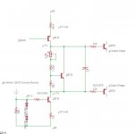
Here is a simplified diagram of the output circuit, with the nominal currents and voltages noted. I would be interested to see what you are measuring both with the load connected and without.
Specifically:
# With no load, and the circuit balanced, what are the voltages across the 0.22 ohm emitter resistors on both sides? This will tell us what the quiescent current is.
# With no load, and the circuit balanced, what are the voltages at the collectors of Q614 and Q616?
This will tell us if you are compensating for some other offset causing source using VR602.
As noted in the diagram, the voltage drop on the emitter resistors should be about 7 mV, implying about 32 mA of current flow. If these are significantly different then this would probably be due to some imbalance in the overall currents flowing on either side.
I am not sure how the bias control is supposed to adjust the overall quiescent current. It clearly is designed to control the offset.
You might find some insights by using a larger load resistor. 8 ohms is so low that it requires heavy currents to drop any significant voltage across it, a nd that may be causing other issues. If you've, say, a 10 watt 100 ohm resistor, then placing that across the speaker terminals shoudl upset the balance, but not as wildly as the 8 ohm load.
You had earlier noted that the offset with the load connected was about -6 volts. If this is in fact the case, then that means the negative side output is sinking 750 mA, instead of 32. That would comprise a voltage drop of 165 mV as opposed to 7 across those emitter resistors.
One possibility is that to compensate for a shorted transistor in the negative side, you are dialing back the bias on the positive side (so with no load, the positive side is current limiting the negative side). When a load is then attached, there is no current limiting, and the negative side draws that full current pulling down the output voltage.
If Q620 and Q622 have very different betas, then this could be the issue. It may be that to get zero offset with no load, you have to adjust the bias all the way one way, and then when a load is connected that imbalance shows up at the load.
This is similar to theory that one of the transistors has an open collector emitter junction, but just not quite as extreme.
Here is a simplified diagram of the output circuit, with the nominal currents and voltages noted. I would be interested to see what you are measuring both with the load connected and without.
Specifically:
# With no load, and the circuit balanced, what are the voltages across the 0.22 ohm emitter resistors on both sides? This will tell us what the quiescent current is.
# With no load, and the circuit balanced, what are the voltages at the collectors of Q614 and Q616?
This will tell us if you are compensating for some other offset causing source using VR602.
As noted in the diagram, the voltage drop on the emitter resistors should be about 7 mV, implying about 32 mA of current flow. If these are significantly different then this would probably be due to some imbalance in the overall currents flowing on either side.
I am not sure how the bias control is supposed to adjust the overall quiescent current. It clearly is designed to control the offset.
You might find some insights by using a larger load resistor. 8 ohms is so low that it requires heavy currents to drop any significant voltage across it, a nd that may be causing other issues. If you've, say, a 10 watt 100 ohm resistor, then placing that across the speaker terminals shoudl upset the balance, but not as wildly as the 8 ohm load.
You had earlier noted that the offset with the load connected was about -6 volts. If this is in fact the case, then that means the negative side output is sinking 750 mA, instead of 32. That would comprise a voltage drop of 165 mV as opposed to 7 across those emitter resistors.
One possibility is that to compensate for a shorted transistor in the negative side, you are dialing back the bias on the positive side (so with no load, the positive side is current limiting the negative side). When a load is then attached, there is no current limiting, and the negative side draws that full current pulling down the output voltage.
Attachments
THE PROF : I shall clarify:
If the amp is switched on is with the speaker/load already connected, then the output goes and sticks at a low of nearly 5--6V. Disconnect and reconnect the load, and the output is restored to zero volts (apparently thanks to the servo action).
What happens when the load is connected (after switch on without load, and now with the output offset at zero) is that the symmetrical voltages at the end of R660 and R662 vary: the negative voltage at the Q622/Q626 end falls to about half the previous symmetrical value. I hope it is clear to you now.
I think I will put Q620/622 on the tester and give them a blast of hot air and see how they behave. Anyway I hope to get a substitute pair (probably A1370/C3476) today or tomorrow so that I could test by substitution.
I had noticed that the original Sanken output devices too had widely differing betas. So did the replacement pairs I had obtained, and which Iam using now. I plan to try and replace them with a pair of OnSemi NJW0281G/0302G, which have exceptional SOA and better NPN/PNP Gain Matching within 10% from 50 mA to 3 A (according to the datasheet) which ought to give us better results here, IMHO. Your advice is important here too.
I shall of course try measurements with higher load resistance and report.
One thing has to be said: the erratic previous behaviour of the L-channel module has improved much and now we are getting some consistent results, leading me to believe that we are "nearly there" as regards the last gremlin or two. I hope to post more systematic voltage readings as per your suggestion. Kindly put up with the incompetence of a harassed lay person scared by the depths he is trying to plumb, though an expert is hand-holding!
I am amused that the Adcom designer's labelling of the bias pot has flummoxed you also. Perhaps we shall explore that angle once the basic issues are solved. As I had stated at the outset, my wish is to disable the DC servo, set the offset manually and then enable the servo as a "belt and braces" arrangement. Once the amp behaves well (the present settling time of 2-3 seconds points to the servo correcting the output offset...?), we could perhaps take up exploring the setting of the offset manually. Then we would also need to find a way to set the quiescent bias too. Kindly keep that at the back of your mind.
COGENIAC : This is interesting. Seems to point to a functional but failing transistor. I suspect, as before, that Q622 id flaky. Are you doing this with or without the servo? If it is with the servo, try it with the op amp out.
The inconsistent behavior is odd, but it is a complex circuit. I suspect that with the load connected the current is high enough to drive the transistor into some odd mode. If it gets started at low current, then it is OK, or we are seeing the confounding effect of the servo.
I'll be interested to see your test results on the transistors and their replacements.
Not sure why it is unable to deal with the load at startup, but we'll figure it out. My guess is that one of the transistors is bad enough that the offset is so high that the servo can't cope with it. Once things settle down, it can.
It also tells me that the offset is load related (which is consistent with my Darlington fault theory).
First thing to do is do the voltage tests with and without a load with the servo disconnected. I think the servo is injecting all sorts of odd behavior into the circuit. The zero output with a speaker connected, disconnected and then re-connected, and subsequent steady state offset at R660 means the servo is creating that offset to compensate for an offset further down the chain.
With the servo out, and no load, adjust VR602 for zero offset at the collectors of Q614 and Q616. Then check the voltages to ground on both sides of R660 and R662. If these are not symmetrical, then you have an issue with one of the Darlington input devices (Q620/622 or Q624/626). If the output stays balanced with no load, then connect your volt meter to one side of R660, and momentarily connect a load to the speaker terminal, and record the voltage on that side of R660. Repeat with the other side of R660. If these voltages are well behaved, then do the same with R662 (this is where it helps to have a high wattage load resistor, so you can sustain an offset for some time).
There are four possibilities:
# If the collector of Q624 is open, then the current to the base of Q628 will be too low, and the negative side will dominate the output.
# If the collector-emitter of Q622 is shorted (possibly with some fixed resistance) then the base current of Q626 will be too high, and the negative side will dominate (this is my suspicion, because you need a lot of current to drop 6 volts across 8 ohms).
# Same case with Q628 and Q626.
I also wonder about your lamps, or whatever you had in the rails. If you put a load in the rail circuit, then that will mask the effect of a shorted transistor. For example, if Q626 was shorted, but there was a series load in the rail, that would limit the current flowing through the transistor, and keep things from going truly bonkers. But it will also mask that fault. So I suggest you remove any rail loads.
It remains to be seen if we need to adjust the overall bias level by changing the current source resistor (R636). I suspect that basic bias level is OK, and the offset is what needs to be adjusted.
THE PROF : In the meantime I got a few pairs of A1370/C3467, with close enough betas, and a few pairs of OnSemi NJW281/302 output pairs, which, again, have close betas, unlike the original Sanken device pairs A1492/C3856.
All the Sanken output transistor PNPs had an average beta of about 120, while the NPNs were down at about 35. Similar values too for the NOS Sanken devices I obtained for replacement. Hence I thought I would move to OnSemi NJW devices, which are far better I gather.
A clarification about my 'protection'--I use a series bulb rated at 240V/60Watts in series with the primary the transformer as I have no variac, which I had found was better than having series resistors in the DC rails. Takes care of shorts/excess current etc and gives you enough time to take measurements.
Today soldered up ONE pair of output devices for testing. Replaced VR602 with a 2k Bourns trimpot. Both rails at 49.5V (with protection bulb in series with the primary of the transformer; no Rs in the DC rails).
Switch on without speaker/load...no 'hunting' of output, as far as visible on the DMM (an analogue multimeter would have been more indicative, IMO). Adjusted VR602 for symmetrical voltages at collectors of Q614 and Q616 (1.56V). No overheating etc, all seems fine. Switch off, connect load of 47 Ohms high wattage R, switch on... very small swing of output which stabilizes in a second or so. Far better performance than earlier with old devices.
Now, switched off, disconnected load; checked symmetrical voltages again, and with DMM at positive end (collector of Q614, top of diagram), connected load --> + voltage rises to near 1.6V. Repeat with DMM at negative end (bottom of diagram) --> the negative voltage falls to about -1.4V when load is connected. This, I think, should aid your diagnostics.
Except for this small discrepancy, everything seems (and sounds!) fine.
But removing the DC servo IC scared me with voltages going haywire, particularly the symmetrical voltages, BOTH going to some negative values, and I switched off without further ado. That part of testing has to wait a bit while we sort out the discrepancy in the symmetrical voltages issue with/without load.
The quiescent current measured across the output device emitter R is very low (just 1 mV or so) with ONE pair of output transistors wired in, and with and without load connected, and with VR602 adjusted for symmetry of the +/- voltages.
Everything now seems/looks/sounds okay, but there is still some niggling issue. What exactly it is, only more testing as per your advice will reveal. I guess for the moment I shall give my poor brain a rest and try to use the amp with a speaker protection circuit, so that regular use might stress some components and hopefully throw up the villain of the piece.
I await your guidance.
COGENIAC : The very low NPN betas were probably your problem. That would unbalance the output and cause it to go negative.
I am guessing that if you let the amp sit for a while with no load, those collector voltages will settle back to being symmetrical. There is no reason if they were set equal before the load was applied, that the balance would change permanently with no change in VR602. I think what you are seeing is that the servo has corrected some offset, and it has a very long time constant.
You might try removing the bulbs in the rails, since the amp is not smoking anything. It is possible that they are not matched, so when a load is applied, one rail falls more than the other, and the servo is compensating for that.
Also, just because it is probably now safe to do so, attach an 8 ohm load, and adjust VR602 for balance WITH the load applied. It is possible that there is some inherent imbalance in the circuit, and setting the balance with a load is different than without a load. Since it is designed to work WITH a load, and it seems to be behaving more or less properly, set it up with a real load and see what it does. I would not be surprised to see, if it was working into a load and was balanced using Vr602, that removing the servo had little effect.
You should also either replace or test Q620, Q624, Q618 and Q622.
THE PROF : Yes, I did put in new devices from Q612 onwards, including ONE pair of NJW281/302 power devices as output devices for testing.
The amp powered up normally (with the protection bulb in series with the transformer primary) and everything was quite close to normal.
But again some gremlin was there. So I tried my 'hot air blast' trick with a focussed jet -- which ultimately brought out the flakiness of Q610--on TWO earlier occasions it had tested and measured well. You learn not to trust out-of-circuit tests!
Replaced it, and things were stable after that!
Now it is going to be the task of wiring in all the three pairs of output devices, putting in a speaker protection relay circuit module, and using the amp for some time as part of extended testing.
It has been one great roller-coaster ride for me, but I enjoyed it thanks chiefly to the patient hand-holding of Cogeniac.
Now that things have come to a satisfactory conclusion, let me say All's Well That Ends Well !
Finally, here is a list of device substitutes that have been tried successfully by myself and others, including our master service sleuths.
It is by no means comprehensive; members are encouraged to add to it and update the list in the course of their adventures with bringing to life an Adcom amp.
The OnSemi output devices with their better PNP-NPN Beta matches at high currents have proved to be robust replacements for the original Sanken output devices, IMHO.
2SA1210/2SC2912 ---> KSA1381/KSC3503
2SA1011/2SC2344 or 2SB595/2SD525 --->MJE15032G/MJE15033G
2SB554/2SD424 ---> MJ21193G/MJ21194G
2SB817/2SD1047 or 2SA1492/2SC3856 (Sanken) ---> NJW3281G/NJW1302G or NJW0302/NJW0281 (OnSemi)
2SC2362 or 2SC2240 ---> KSC1845
2SC536 ---> KSC1815
2SA608K ---> KSA1015
2SA1016 ---> KSA992 or 2SA970
2SA1015/2SC1815 ---> BC550/BC560
DC error amp IC ---> LT1006 or LT1012A or even a CA3130
(E&OE)
- Home
- Amplifiers
- Solid State
- Yet Another Adcom GFA-545-II Restored