Many of us somewhat long in the tooth and who display our gray hairs with pride recall the fondness with which Adcom amplifiers were treated long back. Many of the early amps had the signature of master designer Mr Nelson Pass in their DNA and quite a few models were hot favourites with those who cared for good sound and the ability to drive a variety of speakers well. Recently, after a huge gap of decades, again Adcom gear is finding favour with many and I too acquired a GFA-545-II. Though in non-working condition, I was hopeful of restoring it as a lot of help was available online.
The usual cleaning up of the PCBs, replacement of the electrolytics, checking/replacement of critical components etc breathed new life into it. But the previous owner/service man had tried many things and the amp was not behaving normally. I acquired a copy of the service manual and set out to systematically restore the amp. Soon another 545, in a somewhat worse condition, was acquired with thoughts of cannibalizing stuff for the better of the two. This soon resulted in a working amplifier, but one that had some erratic behaviour.
I had noticed thread where seasoned and experienced Adcom masters were tackling issues with the GFA-565 and posted an SOS there. The resulting exchange is posted here as a new thread. I am also requesting the Admins to delete all the 545-related posts from the 565 thread to do away with the 'thread pollution'.
The posts started with Post #395 on Page 20 on the thread:
https://www.diyaudio.com/community/threads/yet-another-adcom-gfa-565-thread.286742/ :
In order to benefit others who might want to explore working with the GFA-545-II, I am re-posting the entire discussion here in an orderly (though slightly edited) form. Warm regards and much thanks to the masters for all the help.
Last edited:
THE PROF: @cogeniac, Anatech and Phloodpants:
As an Adcom enthusiast, I have been following the thread assiduously for some time. From the early troubleshooting posts, I take it that it is probably best to remove the DC error amplifier IC, and then 'tweak/trim' the LTP so that DC balance is reached, and then restore the error amplifier IC so that a 'nudge' in the right direction will maintain DC balance and keep speaker-killing DC offsets at bay.
I am asking as I have a couple of GFA-545-II models that, over the years, showed erratic and high DC offsets. Replacing the LTP devices cured the issue, but I find that it is possible for the DC error amplifier to "lose grip" due to various factors.
I am banking on your vast experience and expertise to get some sane advice. Is it advisable to replace R616 with a 1k preset and trim the DC balance with the error amplifier IC removed? If not, what should be my approach to trim the DC offset to within the correction range of the error amplifier IC? Kindly help.
It would be great if Sir Scott could find the time to do a detailed "summing up" of his redesign of the bipolar current source (Post # 164), and its integration in the Adcom circuit, for the understanding of many of us who lack the engineering background to follow such stuff easily.
This has been one of the best "educational" threads that I have read in my life (I am a contemporary of Cogeniac!).
My humble salutes to the 'Gurus' !!
Attachments
COGENIAC: Any offsets in the circuit are not a result of diff pair matching. The are a result of the bias circuits over on the right side. I would expect that, since that is all way after any real high voltage gain circuits, your high offset issues may be more to do with some other issues relative to Q614 and Q618.
THE PROF : Yes, I appreciate your idea that adjustability of the tail currents to fine tune the balance is probably the best. I get that regarding your mods to the GFA-565. For me the important thing is the ability to tweak the 'raw' DC balance first, and then activate the servo.
Kindly suggest a way so that I could do that with the simpler circuit of the GFA-545-II. I would definitely like to have a way to null out the imbalances first--with your expert help!
The outputs happen to be triple Darlingtons, which magnifies the errors much!
I have checked the following stage devices and they seem to be working okay, hence my quest for ways to tweak the LTP slightly. Is it advisable to put a trimmer between the emitters, with the wiper going to Q606? Do wise me up, please.
COGENIAC : This is just a hunch, and I do not have the time to spend fully understanding this new circuit, but it looks like the input diff pair is driven by a current source formed by Q606. The base current is set by the two diodes D606 and D608. The actually current is set by resistor R620. I can see why this circuit woudl have a hard time balancing, since it depends almost entirely on some complicated relationship between R161, 618 and 620. If you increase the tail current flow, by reducing R620, then the DC voltage at the collector of Q602 will go down. If your reduce it, the voltage will go up. So, if you are inclined to install a control element to adjust the nominal offset, then adjusting R620 MAY be one approach.
However, I stand by my observation above, that the amplifier is basically single-ended up to Q614 and Q168, so I suspect even changing the bias point of the diff pair may not affect much.
The current balance between the diff pair is not going to affect the DC offset. The triple Darlington is a current amplifier, but it will not actually affect the DC offset unless a device is shorted.
This amplifier appears to be Class A (single ended) up to Q614/Q618. After that some how is changes over to Class B, where one end is driven one way and the other the other way, and getting that balance right is the key, both to DC offset and to crossover distortion.
ANATECH : The balance of the PNP and NPN pairs is not that critical. The balance of each pair is.
PHLOODPANTS : Yeah, I don't try to match the PNP and NPN complementaries. Even if they matched at idle, their curves don't track well.
I build a lot of these boards and I get a consistent -3.8 to 4V correction out of the DC servo to bring the amp to 0V.
PHLOODPANTS : Yeah, I don't try to match the PNP and NPN complementaries. Even if they matched at idle, their curves don't track well.
I build a lot of these boards and I get a consistent -3.8 to 4V correction out of the DC servo to bring the amp to 0V.
COGENIAC : Might help to explain, as much as I understand it, the circuit as it is shown. The differential input pair is a bit like an op amp. The input signal comes in the bas of Q602. Q604 is the non-inverting input. It appears it is there to provide some feedback. The gain of this circuit is roughly set by R616 (which is why a pot there would be bad). The amplified signal comes from the collector of Q602, and goes to the base of Q614. From there it goes out through R648 to some more of the output driver stage (off the schematic). That same signal ALSO goes through capacitor C612, and from there looks like it goes to R650 and off to the negative driver side.
So, up to the output of Q614, there is no positive and negative circuit path, there's only one circuit path. Whatever the bias circuits are for the two transistors (I suspect a 2SC3478 and 2SA1376) is what is going to determine the DC offset. This MAY be affected by the collector voltage at Q614, which may also be affected by Q618 and the circuit with the VR602 pot.
The good news, as I stated earlier, is that unlike the 565, you do not have tons of voltage gain taking small input offsets and amplifying them. The bad news is that this circuit is inherently not very balanced, and so the output stage bias will depend on the bias points of Q164 and the following stages.
ANATECH : It is too bad the diff pair was designed to not balance in many Adcom amps. They depend on the servo, and I think that was a mistake. Notice that the servo is only effective for one polarity of unbalance.
Amplifiers that have a balanced diff pair, or complimentary diff pairs work great without a darned DC servo.
THE PROF : I have put in a pair of C1845s for the LTP, and would like to tweak whatever imbalances there are as a result of the not very close match of the devices. The moment I disable the DC servo, DC balance swings one way consistently. It is this issue that I wish to address-- a way to bring the DC offset closer to zero first, before activating the servo again. Like I asked earlier, is a trimmer between the emitters of the LTP going to help here?
ANATECH : Hi The Prof,
Please read my post above.
The diff pair is designed out of balance, the DC servo is required. This is a weak point and it should not have been designed that way.
THE PROF : @ Anatech:
Sir, can you suggest a way to mod the circuit minimally to make the circuit balance somewhat?
COGENIAC : The interesting difference between the 545 and the 565 is that , since the 565 is full differential Class AB, from start to finish, each side (positive and negative) operates independently. So, introducing a small DC offset to the virtual ground between the positive and negative diff pairs allows control of the overall offset.
The 545 is somewhat different. The bias points of the output stages are interdependent, and may vary according to any of the components in the signal chain.
I suggest trying the R620 pot idea. That will allow you to shift the bias point of Q602 up and down, and that should propagate all the way through to the output stages. Try using a POT for R620. You can use that to turn the bias up or down on Q602, and that will shift the DC voltage at the collector. That shift will propagate through the entire signal path, and should allow you to adjust any offset.
PHLOODPANTS : Yeah, I don't get this, but I still wonder if there was some reason for it, besides the servo. The GFA-535 MKI also has this imbalance in the LTP, and it does not have a DC servo. In both designs, the proverbial "Q1" is the more lightly biased. Could it have something to do with the fact that Q1 supplies drive current to the VAS stage?
COGENIAC : I think that inherent offset is because the inherent beta of the PNP Darlington is lower than the beta of the NPN darlington, so there will always be a slight offset. This is why in the GFA-565 I have used pots for R144/145, so I can adjust that balance exactly. Using 1% resistors in those spots doesn't help, because the NPN and PNP transistors basally need different resistances/currents to yield the same bias points.
The symmetry of the 565 is beautiful, but it's too bad PNP and NPN transistors are not as symmetrical!!
BTW, I am not suggesting anything for the 545, other than using a pot for R620 to adjust the offset. I agree that that circuit is inherently offset, and it is hugely dependent on the bias points throughout the circuit. It looks almost like a classic push-pull output stage that is driven by a single ended class-A amplifier.
In the olden days we would AC couple most of the class-A gain stages, split that signal into two paths, invert one and then AC couple them to the Class-B output stages. So no inherent offset because the output stages were basically biased at zero quiescent current. In the 545 it seems like someone was trying to avoid any AC coupling, and so they worked out all the bias points to make that work. The problem is that ANY error anywhere in the circuit can then upset the whole thing, and errors accumulate as you go from the input to the output stage.
ANATECH : Personally, I strongly believe there is no use for a DC servo if the LPT is matched to begin with. The servo only existed to allow random transistors to be used in manufacture while eliminating an adjustment point. That's all. It was a 100% cost control step.
I watched designs change while doing these products under warranty. There was a strong movement to eliminate the input from technicians to help control warranty program costs. We would list correcting bias and DC offsets in any amplifier we looked at simply because it was the responsible thing to do. Bean counters interpreted that as an added cost when it really wasn't. The reason for the service encounter was sometimes misadjustment, but most often an external issue or baseless complaint. We just avoided future trouble by making certain equipment was properly adjusted. They did the same thing for CD players. Although a fine adjustment often improved a CD player's performance considerably. Often bias currents were way out causing distortion or excessive heat in amplifiers. Offsets could cause a "pop" in preamps and amplifiers.
PHLOODPANTS : Yeah, I think Anatech is right here. If you null out the offset by adjusting the current sources, the output of the amp will still have some offset, and that will drift around a little, but if it's less than 10 or 20mV, no worries at all. Ditch the servo entirely!
COGENIAC : That's an interesting historical perspective....
I definitely agree that if the input sections are balanced properly, offset should not be an issue. There are two concerns, however.
1) Things age, and that will cause the circuit to become unbalanced over time. And the servo can help compensate for that.
2) If there is a failure, the servo can't help, but some sort of servo driven power supply shutdown can prevent applying 85 volts to your speaker terminals.
And, I think you are right, the current source based servo approach seems to be less in-your-ears approach. It basically gets to the real cause of the problem instead of applying a band-aid over it.
I think the best long term solution is to adjust the current sources for optimal offset, and then use the servo to steer them to get the offset to zero over time and temperature. Ideally it will be doing almost nothing almost all of the time.
ANATECH : f your LPT transistors are going out of balance, the distortion will also be rising. A servo hides this, so is undesirable. Besides, this process takes a very, very long time and often things will actually remain in balance.
Call this normal maintenance. You always want the best performance from your equipment within reason. Normally the LPT will remain in balance for 20 years or more. So, why does it need a servo to begin with?
Hafler 220's worked fine without servos (for decades). Any amplifier that used a trim pot (SAE or Phase Linear) didn't normally need frequent adjustment. If you matched the parts, amplifiers I saw a couple decades later were still close.
Marantz and many others with a single LPT and trim pot were also pretty stable.
What I don't like about op amps determining DC offset in amplifiers without speaker disconnect methods is that power up and down instabilities can cause havoc. Call it experience in seeing what can go wrong after you have a few years on something if you want.
Most transistor LPTs don't do funny things as they come up or down, but they can cause thumps for sure. Anyway, there are so many examples of great power amplifiers that did not use a DC servo that there shouldn't be any question as to whether the servo is even necessary. DC servos shouldn't be required.
THE PROF : Couldn't agree more... That brings me to my headache...how to mod the 545 LTP so that it would be "trimmable"... ??
ANATECH : That's what you would call a 'project', because you are really redesigning the power amplifier. But really, the design should be stable, balanced, the way it is as long as the LTP is matched carefully.
What I really didn't like about some of the Adcom amplifiers is that they were designed to be unbalanced, and so require the op amp to work quickly to correct that. I feel that was a massive design error.
The LTP is where the input signal is compared to the output with distortion. The only way the distortion can be effectively cancelled is for the LTP to be perfectly balanced statically. Anything at all that throws the LTP out of balance, such as a DC servo, impairs the ability to extract the difference signal (distortion components) in order to correct it. So in order to make 30 mV of DC offset into 1 mV (for example) you are allowing a higher amount of distortion. So what if you have 30 mV, 50 mV DC offset? That is not harmful to anything. Why trade distortion performance off for something that doesn't matter???
Yes, the LTP is a very basic circuit concept widely used. When you apply it properly the way it was intended it works extremely well. Yes, the current mirror does increase effective gain considerably, but the actual result depends greatly on the load being linear and high-ish impedance. Using a current source increases the common mode rejection a lot. However some people have used fancier current sources to increase the impedance much higher. We run into the law of diminishing returns quickly, so when I encounter a resistor based "CCS", substituting any current source circuit for the resistor increases the performance about as much as you're going to get unless your active CCS is botched. Interestingly, McIntosh used high supply voltages of 130 VDC to 150 VDC and a higher value resistor to achieve a brute force type of high impedance.
As you have seen, the real critical thing is that the two transistors used in a LTP are both matched and the circuit allows them to be balanced. Only then will the circuit perform as expected.
THE PROF : ... I could do with a bit of "hand-holding" from the "circuit surgeons" here... my LTP devices match is not close...all I wish to do is to tweak it manually and leave it there...
COGENIAC : My suggestion for this was to adjust the bias on the LTP so as to move the collector of the LTP output up or down slightly.
From what I can tell, the 545 basically uses the output DC bias of each previous stage to set the bias of each subsequent stage (together with other components.)
The single ended signal finally gets split through an inverting unity gain stage and applied to the output stages. If the DC level of the two signals feeding each side of the Class B output stages is off, then the outputs will reflect that with a DC offset. I think the VR602 POT in the circuit is supposed to control that.
THE PROF : VR602 sets the quiescent bias for the output devices (according to the service manual).
I shall try trimming the LTP tail resistor as you had suggested earlier.
COGENIAC : The DC offset in the 545 arises because the input DC levels at Q619 and Q621 are incorrect. If one is higher than the other you will get crossover distortion AND a DC offset. If they are both too low, too will get crossover distortion, but no offset, and if both are too high, then you will have some Class AB operation (not a bad thing), but too much that and the amp will just be dissipating power as heat and cooking the output stage, since both the positive and negative sections will conduct at the same time.
The match of the input transistors (the LTP) is irrelevant to the offset in the 545. it is critical to the small signal performance of the amp, but it is not apparent that it can cause DC offset. So, if your concern is offset, then forget about the LTP. (but once the amp is working, don't forget to match them, or it may sound like crap).
It appears that Q605 and Q 615 are current sources, stabilized by diodes D105 and D107.
After the circuit involving Q617 (ending at R647 and R 649), the circuit is entirely complimentary (symmetrical for positive and negative sides), so any imbalance between them must be introduced at the point where the single ended signal splits to drive the complimentary output stages.
That split occurs at the collector of Q613. One branch goes to Q619, and the other goes to Q617 (I do not yet understand why Q617 is an emitter follower, since we need some sort of phase inversion at this stage to drive the negative side). I suppose if the input signal swings full positive and then full negative, one side will just go to zero while the other turns on, but man, that's a crappy approach...destined for crossover distortion...
Anyway, it really looks like the trim pot VR601 is there to adjust the bias between the two output sides.
Have you tried adjusting that? Do you know if it is actually working?
If the pot is shot, then you will maybe get some negative cycle swing, but it will be distorted. If Q617 is shot, then you may get some leakage signal through the pot and R643 to drive Q621, but again it will not be the same level as the positive cycle.
Try measuring the voltages at the input side of Q619 and Q621. They should be near zero, and if there is any voltage they should be the same and opposite polarity.
It is important to note that up to the output collector of Q613, there is only one signal path, so there're is no opportunity for any imbalance there. Once that signal path splits, them difference can arise that will result in DC offsets.
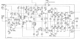
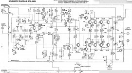
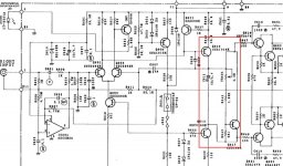
Here is the relevant section of the circuit:
The match of the input transistors (the LTP) is irrelevant to the offset in the 545. it is critical to the small signal performance of the amp, but it is not apparent that it can cause DC offset. So, if your concern is offset, then forget about the LTP. (but once the amp is working, don't forget to match them, or it may sound like crap).
It appears that Q605 and Q 615 are current sources, stabilized by diodes D105 and D107.
After the circuit involving Q617 (ending at R647 and R 649), the circuit is entirely complimentary (symmetrical for positive and negative sides), so any imbalance between them must be introduced at the point where the single ended signal splits to drive the complimentary output stages.
That split occurs at the collector of Q613. One branch goes to Q619, and the other goes to Q617 (I do not yet understand why Q617 is an emitter follower, since we need some sort of phase inversion at this stage to drive the negative side). I suppose if the input signal swings full positive and then full negative, one side will just go to zero while the other turns on, but man, that's a crappy approach...destined for crossover distortion...
Anyway, it really looks like the trim pot VR601 is there to adjust the bias between the two output sides.
Have you tried adjusting that? Do you know if it is actually working?
If the pot is shot, then you will maybe get some negative cycle swing, but it will be distorted. If Q617 is shot, then you may get some leakage signal through the pot and R643 to drive Q621, but again it will not be the same level as the positive cycle.
Try measuring the voltages at the input side of Q619 and Q621. They should be near zero, and if there is any voltage they should be the same and opposite polarity.
It is important to note that up to the output collector of Q613, there is only one signal path, so there're is no opportunity for any imbalance there. Once that signal path splits, them difference can arise that will result in DC offsets.
Here is the relevant section of the circuit:
Attachments
THE PROF : @ Cogeniac:
Much gratitude from my side for your time and effort...I shall study that and act accordingly.
Yes, the Vbe transistor is good and the bias pot is working correctly-- I could set the quiescent current as per recommendation.
The issue basically is once the servo is active, the amp is stable more or less, but swings to a high offset in a random fashion. Once the DC servo is taken out for test purposes, immediately the offset swings negative to about 3-4 V
(I don't have a variac, but I use a multi-watt/multi-bulb/switch combo in series with the primary of the transformer for protection.)
COGENIAC : That description helps. So the issue is not that you can't adjust the bias, the issue is that the bias changes randomly, so the servo is often working, and sometimes cant control it.
It is not worth trying to get the servo to do more. It was never intended for that and as Anatech notes, it should not really even be necessary. You need to find the root cause of the issue. Something us causing the bias on the output stages to go awry.
If you have an amp this is currently in this state, measure the voltage on the input side of R647 and R649. These should be the same but opposite polarity. If they are (or close to it), then the issue is farther down the output stage. it could be a bad transistor that comes and goes, or it could be a flaky resistor.
If these voltages are not equal and opposite, then the issue is somewhere before the output section. Since the output bias is basically set by the circuit includingQ163, Q615 and Q617, check there. The voltage on the diode side of R633 is critical, since it sets the current flow though Q615. If that is off, then the bias on Q613 and Q617 will be off, and that could easily skew the DC levels going into the output stages. This diodes have a forward voltage of 1 volt, so the junction of D607 and R633 should be 2 volts, or very close to it.
You might also check capacitor C611. That seems to be some sort of coupling cap from Q613 to Q617. If that is leaking, then it would also upset the bias balance.
THE PROF : Thanks to you, I have quite a few things lined up.
I am replacing as many of the suspect characters as I can; the previous owner/tech had "tweaked" much, with the result that the amp was running with a high DC offset when I had acquired it. I tried restoring it to the original circuit values.
I know the basics rather well, but undertake complex projects with the guidance of more knowledgeable peers. I had read how an LTP implements negative feedback wonderfully as a differential amp, and one gets to see many such good implementations, both in brands and in DIY. I was obsessed by the DC imbalance and that led me to disabling the DC error amplifier and seeing the raw balance of the circuit. As Anatech has pointed out, the servo seems to be a necessary evil. But then I thought perhaps I could bring the circuit into a narrower 'window' of DC balance first with some manual tweaks/trimming, so that the servo will have a minimal job to do.
I shall attempt to follow your guidelines after I replace some of those critical and interacting devices in a couple of days. I hope to report back good tidings.")
Perhaps Adcom 'specialists' like Anatech or Phloodpants (or even you!) will devote some time to device a good mod for the GFA-545II, which I am sure will take it to another level in performance and, more importantly, long-term reliability.
I am replacing as many of the suspect characters as I can; the previous owner/tech had "tweaked" much, with the result that the amp was running with a high DC offset when I had acquired it. I tried restoring it to the original circuit values.
I know the basics rather well, but undertake complex projects with the guidance of more knowledgeable peers. I had read how an LTP implements negative feedback wonderfully as a differential amp, and one gets to see many such good implementations, both in brands and in DIY. I was obsessed by the DC imbalance and that led me to disabling the DC error amplifier and seeing the raw balance of the circuit. As Anatech has pointed out, the servo seems to be a necessary evil. But then I thought perhaps I could bring the circuit into a narrower 'window' of DC balance first with some manual tweaks/trimming, so that the servo will have a minimal job to do.
I shall attempt to follow your guidelines after I replace some of those critical and interacting devices in a couple of days. I hope to report back good tidings.
Perhaps Adcom 'specialists' like Anatech or Phloodpants (or even you!) will devote some time to device a good mod for the GFA-545II, which I am sure will take it to another level in performance and, more importantly, long-term reliability.
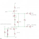
COGENIAC : I spent some time today noodling over the bias control circuit of the 545 amp.
Adcom has a tendency to draw their diagrams rather badly, especially right where the input stage meets the output stage (remember in the 565, this is where that messy bias control circuit is).
Here is the bias circuit of the 545 redrawn. As you can see, the capacitor C611 just passes the signal through from Q614 to Q622, while shielding Q622 from the bias point of Q620 (the collector of Q614).
Q616 is a current source who's current is set by the two diodes in the base circuit. It appears that the current here is about 9.7 mA.
The real party occurs with the little trio of resistors (two resistors and a pot) and Q618.
Because the base emitter voltage of Q618 is always 0.7 volts (nominally), the current through the 681 Ohm resistor (R646) is always about 1 mA. Assuming the base current in Q618 is negligible, this means that the current in the resistor stack is also always about 1 mA. And this means that as the value of the pot changes, the voltage drop across the stack will change. So, when the pot is at zero, the drop across the resistor stack will be .001(1820+681)=2.5 volts, and when the pot is at max, the drop will be .001(2200+1820+681)=4.7 volts.
It also means that the current in Q618 is always fixed as well. Since the voltage drop across R646 (the 681 ohm resistor is the same, and the current through Q618 is constant, that means that the base current in Q618 is also constant, even if the resistance of the pot changes. to accommodate that, the voltage at the collector of Q614 must change as the pot resistance changes. And as the overall equivalent resistance of the resistor stack and Q618 change, the voltage at the collector of Q616 must also change (to keep the current constant).
Exactly how they change is not completely clear to me because the current flow through Q618 and the resistor stack are interdependent.
in a correctly balanced circuit, the input to R648 and R650 should be 1.7 and -1.7 volts respectively. If that is not the case, then the problem is upstream.
Two points:
1) my experience with previous owners is that many of them just fart around trying stuff and in the process end up making things worse. My first 565 had all manner of weird "fixes" that I had to undo before I could even start to get a handle on what was wrong with the amp. So, putting it back to original is a good place to start. Check for leaking electrolytic caps, cold slider joints, fried traces, burnt resistors, etc. I use a nice LED magnifying lamp to inspect the boards and the parts.
2) Caps C611/C612 are not bypass or filter caps, they are coupling caps. they pass the audio signal from one circuit to another while shielding the two circuits from their different DC bias points. If one of them is leaking (as in it has some finite resistance at DC), that will throw off the bias circuit. Probably unlikely, but something to check by lifting one lead and testing its resistance.
Attachments
- Home
- Amplifiers
- Solid State
- Yet Another Adcom GFA-545-II Restored