It's nice to see that there's still an interest and understanding out there of these wonderful devices!
The main problem is that concrete data on the axtual geometry of the VFET/SIT is not at all easy to find. There is some recent work on SiC parts available as patents. Because of this, it comes down to characterizing the various available parts by measuring, and then trying to reconcile with what theory says about it. Some findings so far (like the small positive tempco in high gm devices) are new, but similar to what is found in VMOS. Sony low gm / low capacitance devices exhibit practically 0 tempco, in any case small enough that you can't really tell the sign (although with a lot of controlled statistics it would likely show negative below some current, positive above).
Also, they seem very rugged, and quite overspecified. For instance, both Sony and Yamaha parts often have breakdown voltages 50% over spec. A particular Tokin device capable on paper of withstanding 1kV, had no problems with the full 1.7kV or so of the tracer (and actually behaves amazingly linear at high voltages). A few less known and rare (some so rare that most would believe them nonexistent) devices show that the equally rare published data in tables is not accurate, and some is dead wrong.
SOme findings are surprising and quite perplexing - I have a number of failed devices and some have a very interesting failure mode, which is common even to different manufacturers and types, associated with the G-DS diode failing, resulting in a part with actually VERY desirable charactersitics, a zero bias 'triode' which is very linear andactually has low Ig up to some +2V Vgs or so, but has low gm and breakdown voltage - apparently through the combination of part of the crystal becoming inert (probably burned metalization) and the remaining part becoming doped differently due to current and temperature developed at time of failure.
I'm not sure but what you may be missing the point here.
"Most SITs have Idss approaching the maximum design current as it's the whole idea of a depletion only device. That being said, they also exhibit a small enhancement region when Vgs becomes positive (within limits of a Si diode voltage drop of course), sometimes it actually signifficantly increases Id from the Vgs=0 condition. (*)"
That's exactly how some of the IXYS parts behave. Just like an 811 tube for that matter, a certain value of plate current with a grid voltage of 0V, and the plate current can be driven even higher with a positive voltage.
The data sheet for the 2SK77 does not list a typical Vgs(off) value, but the sheet does state that it is -6V (typical) ~-16V (maximum) on the 2SK75 (shown on the same data sheet). The IXYS part seems to be a bit over -3V (typical).
Cold Triode to replace a V-FET
Zeljko,
nice to meet you again !!
djk might be partially right, at least with a 2SK77 in a B-I, because in B-I, the 2SK77 can't be driven over 0V Vgs, because its 2SK75 driving transistor's drain is connected to the source of the 2SK77.
The Sony datasheets also mention, that the V-FETs can be used as a kind of bipolar, but certainly they are optimized to operate below 0V.
Regarding the gemetry of V-FETs, I can remember to have seen a Yamaha Patent from the early eighties (81 or so) related to their second generation V-FETs (the ones they later used only in electone organs and the GX-1 cabinets) and there they stated some process geometry dimensions and doping concentrations, also of the earlier versions, to prove the difference to the state of the art.
Anyhow, because of lacking 2SK77 replacements, I built my own replacement transistor a few years ago (actually a little circuit around a IXYS IXTH20N50D depletion mode MOSFET), that mimics the following parameters of a 2SK77:
- gm
- mu
- Vgs_off
- Vgs (at B-I bias)
- Almost Zero Tempco (at steady state)
- Cgs (roughly, at B-I bias)
- Cgd (roughly, at B-I bias)
It is obvious, that this stock IXYS part can't be directly used, but with some external circuitry at least at AF you come pretty close.
This was extensively simulated and then proved to work within a real circuit and compared there to a real 2SK77. After some tweaking of parameters I got close, probably less than the production deviations for the 2SK77 (around the operating point as used in the B-I).
Funnily my Cold Triode (TM) even sounded better than the originals in my B-I, so my emulation was probably not as perfect as I thought ...
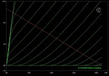
Please find transfer curves appended. IMO more linear than any SiC device or any thermionic triode ... 😀
Cheers,
Mirko
Zeljko,
nice to meet you again !!
djk might be partially right, at least with a 2SK77 in a B-I, because in B-I, the 2SK77 can't be driven over 0V Vgs, because its 2SK75 driving transistor's drain is connected to the source of the 2SK77.
The Sony datasheets also mention, that the V-FETs can be used as a kind of bipolar, but certainly they are optimized to operate below 0V.
Regarding the gemetry of V-FETs, I can remember to have seen a Yamaha Patent from the early eighties (81 or so) related to their second generation V-FETs (the ones they later used only in electone organs and the GX-1 cabinets) and there they stated some process geometry dimensions and doping concentrations, also of the earlier versions, to prove the difference to the state of the art.
Anyhow, because of lacking 2SK77 replacements, I built my own replacement transistor a few years ago (actually a little circuit around a IXYS IXTH20N50D depletion mode MOSFET), that mimics the following parameters of a 2SK77:
- gm
- mu
- Vgs_off
- Vgs (at B-I bias)
- Almost Zero Tempco (at steady state)
- Cgs (roughly, at B-I bias)
- Cgd (roughly, at B-I bias)
It is obvious, that this stock IXYS part can't be directly used, but with some external circuitry at least at AF you come pretty close.
This was extensively simulated and then proved to work within a real circuit and compared there to a real 2SK77. After some tweaking of parameters I got close, probably less than the production deviations for the 2SK77 (around the operating point as used in the B-I).
Funnily my Cold Triode (TM) even sounded better than the originals in my B-I, so my emulation was probably not as perfect as I thought ...
Please find transfer curves appended. IMO more linear than any SiC device or any thermionic triode ... 😀
Cheers,
Mirko
Attachments
Last edited:
The main problem is that concrete data on the axtual geometry of the VFET/SIT is not at all easy to find.
Agreed. In fact any older concrete V-FET data at all is hard to come by. That's why people like me are grateful to people like you and a few others for sharing your findings since you have both an academic interest and you're equipped to experiment with them.
As for me, it's more about the pleasure of enjoying them sonically. Ever since I got my first B-2 I've been completely captivated by how V-FETS work and how wonderful this amp sounds, so much so that I went to the trouble of recapping and extensively reconditioning 2 of them that I rotate between periodically. I find your comparison of the Sony & Yamaha's particularly interesting because just for fun I might try the Sony 2SK82 & 2SJ28 set I have in place of the Yamaha 2SK76 & 2SJ26 in the B-2 since they seem to have quite similar operating parameters.
Attachments


Zeljko,
nice to meet you again !!
And you, Mirko - I would have never guessed it was you based on the nickname here 🙂
I have some new data to share, via PM...
djk might be partially right, at least with a 2SK77 in a B-I, because in B-I, the 2SK77 can't be driven over 0V Vgs, because its 2SK75 driving transistor's drain is connected to the source of the 2SK77.
I'm not in disagreement, it's just the because of the above, one has to count on the 2SK77 providing all the current for the B1's 200W power rating at 8 ohms, with Vgs=0 and reasonably low voltage across D-S. Basically - the maximum current output of the B1 = Id @ Vgs=0 = Idss, so a suitable replacement has to behave the same, AND maintain other important parameters, not the least of which are gate capacitances. While it's easy to increase Idss simply by chosing a larger area device with the same basic geometry, this also increases capacitances and (which might prove even worse) may end up putting the gate at voltages where this capacitance is very non-linear.
The Sony datasheets also mention, that the V-FETs can be used as a kind of bipolar, but certainly they are optimized to operate below 0V.
Yes - in fact every junction FET and therefore junction based SIT/VFET (I'll get to this in a moment *) has an 'enhancement' region, but since the gate forms a diode with the source, you get gate to source current. However, drain current contribution is far more, so there is a kind of BJT-like 'Beta', you could say. The actual limit comes down to how much current the gate-source 'diode' can withstand, and in all the datasheets I have seen, a maximum is specified. This region of operation is almost always used in switching applications to get apparent Rdson as low as possible and minimize losses (note small extra positive supplies for the gate drivers of the class D Sony TA-N88) - Rdson ften becomes half or even less than at Vgs=0V.
The difference with the Russian P-SIT (IIRC this is the name they use) is that it ONLY operates in this region, like a BJT. There is a depletion region but with Vgs=0 the currents are already in uA.
* I searched for the term SIT in old books and found that it was originally the name of a then 'theoretical' device which was in fact thought of before the discovery of the BJT. The basic idea was using a capacitor-like structure over the channel made as a low doped bridge between two high doped areas of semiconductor, in order to attract free carriers and make the bridge more conductive. Of course, little was known about boundary efects between semis and insulation, so experiments required hundreds of volts for very little current differences. It seems the 'Static Induction' terms refer to this. Note that in principle this device is what we now call a MOSFET but more properly termed IGFET or insulated gate FET. It also seems that the creators of the original VFETs called them that rather than SIT. On the other hand, in principle you could create similar behaviour (triode-like) in MOSFETs, but so far there is no process developed that would produce the required geometry.
Regarding the gemetry of V-FETs, I can remember to have seen a Yamaha Patent from the early eighties (81 or so) related to their second generation V-FETs (the ones they later used only in electone organs and the GX-1 cabinets) and there they stated some process geometry dimensions and doping concentrations, also of the earlier versions, to prove the difference to the state of the art.
These are quite different than the original 2SK77/76 series. There also seems to be a large discrepancy between published data (what little there is) and actual performance, but that's a different story altogether.
Anyhow, because of lacking 2SK77 replacements, I built my own replacement transistor a few years ago (actually a little circuit around a IXYS IXTH20N50D depletion mode MOSFET), that mimics the following parameters of a 2SK77:
- gm
- mu
- Vgs_off
- Vgs (at B-I bias)
- Almost Zero Tempco (at steady state)
- Cgs (roughly, at B-I bias)
- Cgd (roughly, at B-I bias)
It is obvious, that this stock IXYS part can't be directly used, but with some external circuitry at least at AF you come pretty close.
This was extensively simulated and then proved to work within a real circuit and compared there to a real 2SK77. After some tweaking of parameters I got close, probably less than the production deviations for the 2SK77 (around the operating point as used in the B-I).
Funnily my Cold Triode (TM) even sounded better than the originals in my B-I, so my emulation was probably not as perfect as I thought ...
Please find transfer curves appended. IMO more linear than any SiC device or any thermionic triode ... 😀
Cheers,
Mirko
And more linear than the original 2SK77! In fact, based on 2SK77 curves, your replacement performs signifficantly better so I'm not surprised at your observations re sound.
YAMAHA B1 AMP 2SK77 Suppose I were to say that all four VFETS seem to check out just fine. I've got more than 5 meters and they don't agree with each other! I know check the batteries and the test leads, zero it out and how does the diode test function? I get about 1/2 ohm between source and drain then my patience runs out with the other tests and results. I got a fellow DIYer that can use it for parts but what is its real value?
YAMAHA B1 AMP 2SK77 Suppose I were to say that all four VFETS seem to check out just fine. I've got more than 5 meters and they don't agree with each other! I know check the batteries and the test leads, zero it out and how does the diode test function? I get about 1/2 ohm between source and drain then my patience runs out with the other tests and results. I got a fellow DIYer that can use it for parts but what is its real value?
Set your meter for its diode test function. The readout in this mode is in volts. Connect the positive meter lead to the Gate, and the negative lead to the Source. You should read about 0.590V (590mV). Now remove the meter lead from the Source pin and attach it to the Drain (the case of the device). You should read about the same here as you did when measuring from the Gate to the Source.
When it comes to the "real value", that's hard to gauge but from what I've seen, even a non-functioning B-1 can fetch big dollars from someone who wants/needs one as a donor unit to support their functioning B-1 or fix their non-functioning one; there are lots rare and unobtainable parts that can only be found in another B-1.
I think it is very difficult to replace K77 with other device.
Their K77 works as common source amplifier.
They are not quasi complementary or drain common (source follower) or D-G feedback (like tubes' anode-grid FB).
So their gain is feedbacked to input stage.
Then, to replace it, you must reconsider compensation...
Their K77 works as common source amplifier.
They are not quasi complementary or drain common (source follower) or D-G feedback (like tubes' anode-grid FB).
So their gain is feedbacked to input stage.
Then, to replace it, you must reconsider compensation...
I think it is very difficult to replace K77 with other device.
Their K77 works as common source amplifier.
They are not quasi complementary or drain common (source follower) or D-G feedback (like tubes' anode-grid FB).
So their gain is feedbacked to input stage.
Then, to replace it, you must reconsider compensation...
That's somewhat inaccurate but largely correct, it's a 'SEPP' arrangement where the diving voltage is bootstrapped to each source.
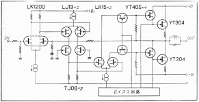
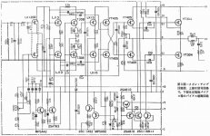
I'm attaching two images to this post, the basic topological layout of the B1 in the first, and the actual schematic in the second, this is from the prototype documentation.
For reference, YT-405 was the original prototype marking of what was later to become the 2SK75, and YT-304 was the prototype for the 2SK77, although the YT-304 had a bigger die and was capable of drain currents up to 30A, whereas the 2SK77 is slightly reduced to 20A, with corresponding reduction of the input capacitance (which was most probably the reason for the reduction).
As can be seen, it's a triple differential design, with the last differential stage cascoded from a rather high negative voltage rail in order to provide the necessary negative bias to the output stage. The ouptuo stage itself is a VFET 'darlington' which means the negative bias voltages of the 'darlington' stages add up to quite a few volts. The important bit is that the gates of the 'darlingtons' are connected through resistors to the corresponding ;darlington' source, so the voltage between the gate and source of the VFET 'darlington' combo can at most be zero. The 'darlington' drivers CAN actually drive the YT-304 (2SK77) into a positive gate region but the current is inherently limited not only because of the series 39 ohms resistance, but also because any positive voltage on the YT-405 source, while the total 'darlington' gate-source voltage is zero, means the YT-405 sees by itself a negative Vgs, limiting the current. On the actual schematic we can also see that the YT-405 that are in the VFET 'darlington' have their sources pulled to a negative rail through current sources.
Although the whole thing does look symmetrical and the top and bottom half of the totem-pole outputs have their driving voltages referenced to their respective sources, this does indeed suggest (and bes describes the operating mode as) common source connection. But there are a few points which make the output slightly asymmetric - for one, the upper half provides current for it's driver (as it comes from the output) whereas the bottom half driver current comes from the output stage negative power rail. Although the driver stage itself is cascoded, the cascode elements are VFETs, which have a triode characeristic, so their gain/transconductance depends on Vds, which is different for the upper and lower half driver - constant for the lower half since it's referenced to the output stage negative power supply, and variable, but on average higher by the magnitude of the output stage negative power supply, for the upper half driver. Because of the cascode arrangement this does not manifest itself greatly but it's still far more present when compared to pentode characteristic devices in the same place.
Neither of the above 'asymmetries' are really a big problem in practice. and are more of the academic kind, but I mention them here because they are actually typical of topologically similar tube designs, for instance a Futterman OTL.
Attachments
Last edited:
Zeljko,
I know you are a secret guy ... but, from where do you get prototype documentation for the B-I ??? 🙄
Then you also have a mask set ??? 😀
I know you are a secret guy ... but, from where do you get prototype documentation for the B-I ??? 🙄
Then you also have a mask set ??? 😀
Zeljko,
I know you are a secret guy ... but, from where do you get prototype documentation for the B-I ??? 🙄
Then you also have a mask set ??? 😀
Sadly no ;(
The schematics and quite detailed development data was published in 'Radio technology' magazine in 1975, January issue.
Is it a magazine from follow URL ?Sadly no ;(
The schematics and quite detailed development data was published in 'Radio technology' magazine in 1975, January issue.
Radio magazine - The Radio Broadcast Technology Leader
Obviously not listed about
http://www.diyaudio.com/forums/soli...ently-available-electr-audio-magazines-2.html
Obviously also still available like this:it seems to be japanese magazine ラジオ技術(radio-gijutsu).
http://www.diyaudio.com/forums/soli...sen-jikken-yearly-index-1924-2009-wanted.html
Attachments

Generally, "radio gijutsu" have more technically advanced articles than "MJ".
But radio gijutsu is more minor than MJ.
There is no indexes on the internet as far as I know.
But radio gijutsu is more minor than MJ.
There is no indexes on the internet as far as I know.
Hello Downandy
Extenders board is made to have possibility to make easy mesurment on any component on the suspected board :
I don't know how to insert an image but you can email me by pm and I will send it to you .
I have refixed some B1 and many B2 some C1 also , I will help you with pleasure. I can refix your boards if yuou send them to me . I have 3 b1
Best regards
QUADESL63
Thank you for your reply. I've done some work on mine and keep getting closer to fixing it. I'll send you my notes in a follow up email. I'm just wanting to get rid of it now. talk to you soon
andy
andy
I'm just wanting to get rid of it now.
I can help you out with that.
 😀
😀QUADESL63 and all
After relearning how to use my DMM, I’ve tested (and retested yesterday) my 2SK77 VFets and they are all good.
I’ve learned the process to discharge my capacitors with a 8 ohm 250 watt Dale resistor.
I have replaced all the electrolytic capacitors on board three then found a blown transistor TR699 replaced it and another (TR703 nearby) checked my faulty -200 V B+ and remedied that problem, with good readings on the 45V,12V and 25V +- power supply.
Turned it on and listened to some very nice Jazz from a local college station, for about 10 to 15 minutes. ! noticed that the left side was heating up and it finally shut down on thermal protection.
Found another bad transistor and replaced TR503.
Made a short test afterwards and the unit still works.
Now I blow the 5A input fuses .
- Home
- Amplifiers
- Solid State
- YAMAHA B1 AMP 2SK77