Hi Elso, so you don't use a shielded cable for output ? If I understand correctly you use just 1 wire for output or a shielded cable with ground disconnected at one side ?
One Wire Only
Jean-Paul,
I am using one wire, as short as possible, for the clock output, not coax.

jean-paul said:Hi Elso, so you don't use a shielded cable for output ? If I understand correctly you use just 1 wire for output or a shielded cable with ground disconnected at one side ?
Jean-Paul,
I am using one wire, as short as possible, for the clock output, not coax.
Re: fmax measures
Correct, and you can always take the ac supply if you don't have space for a transformer.
On the PCB, I suggest you have as small a pcb as possible to take advantage of the small size regulator. Mount this on a ground plane as before, and you end up with a very easy to mount unit
------------------------------------------------------------------------------pedro said:Fred,
Was not "8 to 10 nV/Sqrrt Hz" the noise you get when you made the measures within the TL1763?
Something more:
Could any of you advise on the design to build a psu with a separate trafo, instead of using the supply from one of the regulators in the CD player?
Pedro.
Correct, and you can always take the ac supply if you don't have space for a transformer.
On the PCB, I suggest you have as small a pcb as possible to take advantage of the small size regulator. Mount this on a ground plane as before, and you end up with a very easy to mount unit
separated trafo
Jean Paul,
What I'm actually using is:
Taking +V from the filter caps in the cd-player supply, using a unshielded teflon wire of about 15 cm; a 3cm. single teflon wire to the cd-player ground board and another 3cm. wire from the XO output to the cd-player place where the signal has to be solder.
Within the next days I'll test a separate trafo, and I'll tell you what I find.
I the case of a separate trafo psu: what kind of gnd connection do you recommend?
Anyhow, I really would like to know what sort of filtering is Guido using in his supply for the separated trafo, I mean: where does he place the choke he uses and how many mH is he using.
Re: Re: schematics
Hi
Pedro is showing us true decoupling 🙂
I suggest, assumed you have a decent regulator on the PCB, to use only 1 gnd wire, and to twist that with the clock outpu. The + is a single wire, where only DC runs
Pedro, for the last mm, you can still reduce the loop by going as direct as possible from + of decoupling to pin 8.
In your last layout you make something that the americans call a U-turn
succes
jean-paul said:
That's what I call a short circuit ! Please have a closer look at the PCB and you'll see what I mean. Pins 8 and 4 ( 5V and GND ) are shorted. The layout in post 11 was better except for the location of the 47 uF OSCON.
When an internal supply is used there is a possibility that the ground via the clock board will be a lower impedance "bypass" of the ground path of the cdplayer ( as experienced by me with various Philips cdplayers ).
Hi
Pedro is showing us true decoupling 🙂
I suggest, assumed you have a decent regulator on the PCB, to use only 1 gnd wire, and to twist that with the clock outpu. The + is a single wire, where only DC runs
Pedro, for the last mm, you can still reduce the loop by going as direct as possible from + of decoupling to pin 8.
In your last layout you make something that the americans call a U-turn
succes
to fred
Fred,
Thanks for your reply too.
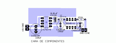
How do you find this actual psu design: the TL1763 LDO mounted in the adaptor (brown dog) and soldered as here, with all this groung plane around.
My problem is that I don't have all those devices all of you use to measure noise.
I only can say that with this board, being more or less like the one shows here, not short circuited;-) the sound is really very good. And, of course, no ground loops or hum at all.
Fred,
Thanks for your reply too.
How do you find this actual psu design: the TL1763 LDO mounted in the adaptor (brown dog) and soldered as here, with all this groung plane around.
My problem is that I don't have all those devices all of you use to measure noise.
I only can say that with this board, being more or less like the one shows here, not short circuited;-) the sound is really very good. And, of course, no ground loops or hum at all.
Re: to fred
If it sounds good, that is the ultimate test!

--------------------------------------------------------------pedro said:Fred,
Thanks for your reply too.
How do you find this actual psu design: the TL1763 LDO mounted in the adaptor (brown dog) and soldered as here, with all this groung plane around.
My problem is that I don't have all those devices all of you use to measure noise.
I only can say that with this board, being more or less like the one shows here, not short circuited;-) the sound is really very good. And, of course, no ground loops or hum at all.
If it sounds good, that is the ultimate test!
I plan on building the PSU that Pedro presented.
Is it ok to make the leads as wide as possible or should I stick with the original PCB design?
Where do I find a list of component dimensions. I plan on drawing a few very simple PCB's and I plan on using Powerpoint for drawing (I don't wan't to take time to learn how to use a complicated program right now).
Attachments
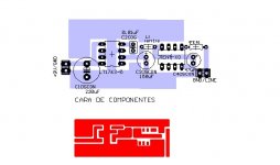
I desided to try the PSU that is recommended by Tentlabs. How does this layout look like?
Does anyone have an image of a tentlabs PSU PCB? I could try to make a decent PCB for PSU but I don't have any software for drawing one. PCB image would be gratly appreciated!
Does anyone have an image of a tentlabs PSU PCB? I could try to make a decent PCB for PSU but I don't have any software for drawing one. PCB image would be gratly appreciated!
Attachments

DIAR said:I desided to try the PSU that is recommended by Tentlabs. How does this layout look like?
Does anyone have an image of a tentlabs PSU PCB? I could try to make a decent PCB for PSU but I don't have any software for drawing one. PCB image would be gratly appreciated!
Hi
Just to clarify: The circuit I recomend differs from the circuit present at XO2 and XO3
The DIY circuit is critical at cap location around the 7808 (these should be close to the regulator), and ofcourse the decoupling around the XO. The rest is fairly easy and sub critical.
cheers
Thanks Guido!
I tried to put the capacitors as close to XO and Regulator as possible. Maybe I'll find a way to place them even closer.
A friend of mine suggested I should add a small value ceramic capacitor to XO output to reduce possible harmonic frequencys of XO. Any opinions on this?
EDIT: I was thinking about placing the PCB into a well shielded metal enclosure. Or is it unnecessary?
I might move the voltage regulator away from the electrolytic capacitors as heat shortens their life. A couple more centimeters won't make much of a difference electrically.DIAR said:I desided to try the PSU that is recommended by Tentlabs. How does this layout look like?
DIAR said:
A friend of mine suggested I should add a small value ceramic capacitor to XO output to reduce possible harmonic frequencys of XO. Any opinions on this?
I take this back. Just a little misunderstanding. He suggested I should add a small ceramic capacitor next to the 0.1 uF cap near the XO. Makes more sense. 😀
Edit: Now I'm totally confused. I saw a schematic with small ceramic cap in series with output 😕
I've been thinking about the heat problem, John. I desided to change the heatsink to an aluminum bar or L-profile. I wonder how hot the regulator will become... Atleast the current is very small.
DIAR said:
I take this back. Just a little misunderstanding. He suggested I should add a small ceramic capacitor next to the 0.1 uF cap near the XO. Makes more sense. 😀
Edit: Now I'm totally confused. I saw a schematic with small ceramic cap in series with output 😕
I've been thinking about the heat problem, John. I desided to change the heatsink to an aluminum bar or L-profile. I wonder how hot the regulator will become... Atleast the current is very small.
Hi
Do NOT place the parallel cap, a special RF cap is integrated in the XO
The series cap is not realy required
One other note: With 5V on the supply, the XO puts out 5V clock. When the original clock chip is running at 3.3V (check power suppl), the output can be reduced by lowering the XO voltage: The most simple way to do so is lower the 56k resistor to 22 k
best regards
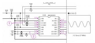
DIAR said:Good that you mentioned the voltage issue. According to CDP service manual, klock input is only 1.6 V so I have to lover the voltage quite much.
Hi
The chip runs at 3.3V, so the XO should run at 3.3V too. The suggested change will do the tricjk
regards
I'm going to connect the module to CDP PCB using about 10 cm long Raydex RG316 cable:
http://www.farnell.com/datasheets/47409.pdf
It is probably not the best possible cable for this application but I have it at home and couldn't find any better in local stores and I don't wan't to order a 100 meter reel.
I'm thinking about soldering the cable (ground and signal) to CDP PCB and connecting the cable to clock pcb by using these connectors from RS:
http://www.rsfinland.com
straight plug RG178 245-5058 €3.60
right angle thru hole skt 245-5137 €5.30
I use connectors for easy disconnecting and modification of the clock module. Hopefully those connectors are ok...
Guido Tent said:Do NOT place the parallel cap, a special RF cap is integrated in the XO
I'm a bit 😕 Guido,
On your XO2, There's clearly an external cermamic capacitor for the 5Vdc supply on the pcb...or has that been obsoleted in more recent revisions ?
- Status
- Not open for further replies.
- Home
- Source & Line
- Digital Source
- XO powersupply PCB board diagram