there is already an answer from Nelson….
look here
http://www.diyaudio.com/forums/pass...gle-ended-current-sources-29.html#post4217800
look here
http://www.diyaudio.com/forums/pass...gle-ended-current-sources-29.html#post4217800
For now I leave it as an exercise for the DIYer to go through the permutations of resistors in the feedback networks. With the blessing of Papa I will show the configuration that produced the plots in posts #348 and #349.
Hello lhquam. You are demonstrating an impressive mastery of LTspice and of other core electrical subjects. Admirable.
I revisited post# 207, and recalled my excitement hearing the performance of the DIY amp therein; which you had partly proposed. It is possible that its subjective performance maybe related to that expected of your prototype amp under study.
Connections..part1
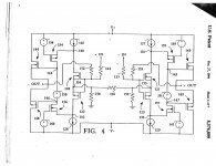
The image shows an example schematic of a Super Symmetric Amplifier which was invented and taught by Nelson S. Pass in US Patent #5,376,899. I'll highlight the following observations by focusing on the right-side schematic which receives an AC signal at the -IN input port. These observations full apply to the left-side schematic which is a mirror image of the right-side one.
1. The circuit topology which is attendant to the Mosfets labelled 121, 123 [front end], 135, and 137 [folded cascode] may remind of the LSK Preamp shown by Mr. Pass at BAF 2013.
2. The power output stage Mosfets are complementary symmetry. The N-channel is labelled 145, and the P-channel is labelled 149. These single units may be several N-Mosfets or X individual units, and several X individual units of P-Mosfets. May remind of the power output stage of diyF4.
3. Feedback from the +OUT port is returned via resistor 153 to the joined gates of the front end Mosfets. Feedback allows the joint sources of this front end Mosfets to communicate the distortion emanating at +OUT with/to the left-side schematic via the bridge resistor [156] for out of phase cancellation.
I can readily perturb Super Symmetric Amplification and the attendant attributes of this schematic as follows:
1. Use X units of N-Mosfets and X-1 units of P-Mosfets in the power output stage of the right-side schematic.
2. And simultaneously use X-1 units of N-Mosfets, and X units of P-Mosfets in the power output stage of the left side schematic.
The resultant schematic lost Super-Symmetry. I understand from the clear logic,and flow of ideas in this thread that its or similar practical power amplifier is rich in the second harmonic which is profoundly valuable for its subjective performance.
In a following logical step, a technical need has emerged to manage, and/or dial to suit the levels of the beneficial harmonics of a practical amp so as to bring out its best performance. This brings me to the recent LTspice schematic written by lhquam. It has the basic working elements of the above Perturbed Super Symmetric schematic. He further teaches tweaking the levels its expected resultant harmonics [H2 dominant] by using the novel circuit/approach by Mr. Pass which Pass called Cascode Feedback.
Part 2 will examine the LTspice schematic written by lhquam so to learn about Cascode Feedback.
Connections ...Part 2.
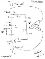
The image shows a very simplified schematic of the Right-Side amp of lhquam's LTspice schematic of his balanced amp which has appeared in previous posts. Please note the following.
1. The left side of the image shows the schematic of the front-end [FE]. It is comprised of precision matched complementary symmetry JFETs, which are further "cascoded" with precision matched complementary symmetry bjts. This FE is highly symmetrical. Note the idle drain current bias .
2. The outputs of this FE appear at the collectors of the bjts, and find their way to the asymmetric power output stage [APOS] which is shown on the right-side of the image. APOS is well defined in lhquam's schematic.
There are three distinct, or unique, or singular [meaning not redundant] methods to lower the distortion of this amp.
1. Overall loop feedback starts at the -OUT port and terminates at the joined sources of the FE's JFETS. The resistors 4.7K and 220 Ohms further define the closed loop gain of this non-inverting amp.
2. The 220 Ohm esistor which is connected the joined souces of the JFETS is the bridge which communicates the distortion of this amp to the Left-Side amp so as to reap the benefit of lowering further the distortion via the unique mechanism which is embodied in Super Symmetric Amplification
3. The third method is Cascode Feedback. The emitters of the cascoding bjts are connected as shown in this image to the -OUT port, and conform with/to lhquam's schematic.
Let's talk Cascode Feedback [CF] which is I present as qualitative, simplistic and descriptive. The benefits of the cascoding bjts are well established and are highly valuable; like shielding the JFETS from Vds fluctuations, and safeguarding them from undeserving thermal stresses. One needs to further view the cascoding bjts as solo common base amplifiers which bring to this table these additional attributes:
1. Wide-band
2. Highly linear
3. And the emitter port of the CB amp has a low impedance which is highly useful to sum currents from several sources without cross interactions or affect among these sources.
Offer the -IN input a negative going signal. At its negative peak [shaded for example], the channel of N-JFET is choked a bit such that a [delta i] loss from its idle current is perceived. Simultaneously the -OUT port signal also goes negative [non-inverting amp]. At its negative peak, it channels or siphons a [delta i' or redirects the aforementioned delta i ] current through the upper cascode feedback branch. Here's the point. The common base NPN sums these out of phase currents [delta i and delta i'] and their net sum flows across the NPN's collector load resistor. The new voltage drop [after CF versus before] flows across the load resistor of NPN and is sent to APOS for recycle.
Simultaneous to the above happenings, an apposite situation occurs on the P-JFET side. Again the PNP common base "cascode" amp maybe seen as summing two out of phase currents at its emitter; which is a corrective; distortion lowering negative [valuable] feedback.
The above happenings are also on-going in the Left-Side amp of lhquam's LTspice balanced amp schematic. Now wrap your arms around this bigger picture of the concurrent use of these 3 singular methods of error correction in it.
I may need a Part 3 to tie up loose ends in my thinking.
Attachments
Connections...Part 3
The LTspice schematic of the balanced amp by lhquam, and the rich rapport in past posts have sparked the following ideas:
1. Use complementary power output stages in it instead of the asymmetric ones he described. The resultant is a schematic for a hypothetical Super Symmetric amplifier which is expected to have very low %THD distortion; if any can be detected; because it uses a total of 3 singular methods of error correction/reduction therein. This approach maybe further extrapolated to pre-amplifiers which have a topology basis of Super Symmetric Amplification.
2. Use in power amplifiers which are not balanced. DiyF5 comes to mind which in this idea has a cascoded front end. This modified diyF5 maybe operated by using the cascoding bjts in the passive [shielding] mode, or preferably give'm the added responsibility per the scheme of lhquam so as to further diminish the %THD of the parent amp.
Best regards.
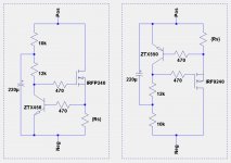
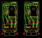
experimental CCS PCB
I have been experimenting with constant current sources in an amplifier similar to a BA-3b(balanced) that has some similarities with the XA30.8. After building for a particular configuration of active output FETs and CCS fets I discovered that my output stage PCBs didn't have all of the flexibility that I need for experimentation. I came up with a way to easily modify those PCBs by making it possibly to reconnect one gate resistor of each quadrant of the output stage so that each quadrant can have either 4 or 5 active output FETs.
The CCS circuit is a 2-terminal circuit connecting a output phase to a power rail whose output current is controlled by a single resistor Rs. The CCS is placed on a tiny PCB that mounts to a spare location of the heatsink using the same screw that attaches the CCS mosfet to the heatsink. Using 2 such circuit boards, and 4 wires one can experiment with an combination of quadrants for the CCS.
Show is a photo of a perf. board prototype of a CCS using an IRFP9240, and the schematics and PCB layout for current sources of both polarities.
Attachments
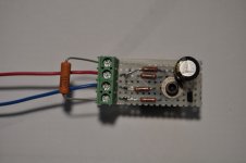
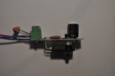

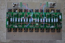

I forgot to mention that all of the red and blue wires have female connectors for square posts used in standard cable headers. Each quadrant can have 4 or 5 active FETs by replugging 4 of the wires attached to gate stoppers. Each CCS can be configured for either the positive or negative rail by replugging two of the wires. The CCS currents are determined by the resistors in the Molex connectors.
All that remains is exhaustive listening every possible configuration of everything including the active FET bias currents and the listening material, ...
Isn't that what Nelson had to do? 😀
All that remains is exhaustive listening every possible configuration of everything including the active FET bias currents and the listening material, ...
Isn't that what Nelson had to do? 😀
I was a bit tired of the search for the right k2 for the Toshiba SK/SJ Mosfets
And simply put in instead, the good old IRF 9610-610 combo and kept the same load and driver bias.
The SE bias arrangement was the resistor solution the .5 uses.
Not as dynamic, neutral and clear as the Toshibas, but so coherent and involving that I decided to make a break with the Toshiba drama searching for correct values for CCS to get enough k2 to have appropriate body.
😀😀
No, I changed one year ago to Tannoy and at the moment I enjoy parallel to Tannoy old Klipsch Forte II
not bad……
where is the progress?
😀😀
not bad……
where is the progress?
😀😀
- Status
- Not open for further replies.
- Home
- Amplifiers
- Pass Labs
- XA.8 single-ended current sources