Hello
An old thread coming back.
I did not follow all the thread, but I can reply about the VAS not responding quickly enough.
In my amps I use a low value Miller compensation capacitor and also a phase lead capacitor to keep the amp stable. So I get a better slew rate and a faster VAS.
So Tessier, for his amp in post #54, should reduce the Miller compensation capacitor to 17 Pf and add a 10 Pf capacitor between Q7 collector and Q4 base (it's a phase lead capacitor), and he also should do as Hugh suggested for the drivers current.
Bye
Gaetan
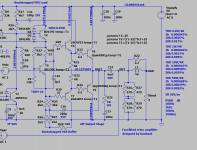
My bootstrap amplifier, tested:
https://anistardi.wordpress.com/2014/04/19/aksa-55-dalam-simulasi/
https://anistardi.wordpress.com/2014/10/14/perkutut-amplifier/
With current mirror on LTP and 2EF VAS, it can achieve high open loop gain then it can use TMC or TPC compensation. THD will very low at all audio frequency with H2 dominant 😎
I don't know if H2 dominant is important with such low THD.
That´s a very broad statement.I understand that a diode is not good in the way of the audio signal.
Consider that each BE junction IS a diode and IS in the signal path ... dozens of them in any System.
Thanks for answering.That´s a very broad statement.
Consider that each BE junction IS a diode and IS in the signal path ... dozens of them in any System.
I understand. But I was referring to the differences between transistors and diodes. As far as speed, cob, noise..........
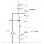
1. The purpose of the diode in the bias network is to improve the negative swing, i.e. cancel the VAS saturation voltage. But it should be decoupled with a capacitor across the whole bias circuit so that it does not add distortion. But actually, such a capacitor is a form of (double) bootstrap that allows the VAS to drive below the negative rail and without the issues with a BS from the output.
2. A BS and a CCS are not mutually exclusive. The lower resistor can be replaced with a CCS, which ~prevents the BS from exaggerating crossover distortion.
3. Driving the BS directly from the emitter avoids the signal loss of the emitter resistor, and/or the output EF, but it is not good for crossover distortion since the positive feedback will be distorted.
4. Many BS circuits use two matching resistors because that is the highest total load resistance on the BS capacitor and therefore the lowest effective frequency, but this means that the VAS output can exceed the rail by half the supply voltage, which tends to create rail sticking. The TL431s in the double BS circuit are there to limit the BS voltage for this reason. A simpler method is just to reduce the lower resistor so that the BS voltage is limited. An alternate is a clamp to the upper rail.
5. Turn on thumps are more likely because there is no current mirror on the LTP and therefor the VAS has no input until the LTP current reaches full current. Thumps happen when the LTP shuts down while the VAS is not. A diode can be used to quickly pre-charge the BS capacitor quickly. The lowest effective frequency of the BS is just a matter of the cap value vs the BS resistors.
6. A partial BS is a good way to drive the OPS to saturation for best efficiency while avoiding stability issues and avoid rail sticking.
7. Bootstraps is a common way for class-D amps like the UCD to drive the upper gate above the positive rail.
Steveu, you say:
5. Turn on thumps are more likely because there is no current mirror on the LTP and therefor the VAS has no input until the LTP current reaches full current. Thumps happen when the LTP shuts down while the VAS is not. A diode can be used to quickly pre-charge the BS capacitor quickly. The lowest effective frequency of the BS is just a matter of the cap value vs the BS resistors.
To understand better, do you have any circuit diagram? (A diode can be used to quickly pre-charge the BS capacitor quickly)
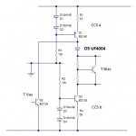
The diode serves two purposes. Originally it was used with a double bootstrap drive in a Mullard circuit so that the driver stage can swing to a greater voltage than otherwise; the second was to provide a protection for the VAS transistor in the event of a short circuited output. In the circuit in post 88 only the second advantage is possible as the CCS's limit the voltage swing rather than bootstrapped resistors.
There is no good reason to use a transistor here. The impedance of a diode biased in the forward direction is in the region of a few ohms that will have almost no impact on the high output impedance from the ccs. There is a danger that a transistor could be reverse biased beyond its Vebo (typically 7V, usual spec. 5V) with a shorted output, but a diode will withstand 100V or so (1N4004, 400V). If you want a fast response for better protection one of the UF device range might be a better choice.
There is no good reason to use a transistor here. The impedance of a diode biased in the forward direction is in the region of a few ohms that will have almost no impact on the high output impedance from the ccs. There is a danger that a transistor could be reverse biased beyond its Vebo (typically 7V, usual spec. 5V) with a shorted output, but a diode will withstand 100V or so (1N4004, 400V). If you want a fast response for better protection one of the UF device range might be a better choice.
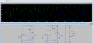
I had to revisit this and simulated several circuits, but while they worked, most had issues so here is a comparison of a typical BS and one with a quick start that works. I'll spare you the circuits that have problems. The issues with the other simpler circuits drives home the point that this is probably not worth doing so you do not see it in commercial products.To understand better, do you have any circuit diagram? (A diode can be used to quickly pre-charge the BS capacitor quickly)
I think the point of a BS is to avoid the need for extra power supply voltages. Unless you have done some circuit design, the need for extra bias voltages may not be familiar. It reminds me of the logic voltages of TTL vs CMOS. TTL logic zero is about 0.5V and a logic 1 is about 3.0V, out of a 5V supply, because TTL is made with NPN bjt transistors, so there is a significant bias voltage problem driving a logic 1. Are you old enough to remember memory chips that required multiple supply voltages? Today everything is CMOS. One reason CMOS is so power efficient is that the gate voltage fits nicely within the main two supply rails. Likewise, if our amplifiers use common emitter/source outputs, there is no need for bootstrapping or extra supply voltages.
Attachments
Last edited:
I'm getting the impression that you might actually know the answer.
But I'll reply anyway.
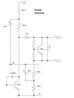
Any load resistor for a transistor will limit the current available as the voltage swings towards the power rail. For example: amplifier with +/-30V rails and a 2k load resistor will need the VAS to pass 30/2=15mA standing current. Let the transistor turn off, the voltage rises. If the driver and output transistor combined gain is, say, 500 then for 5A output the base current needs to be 10mA. A 2k resistor will limit the voltage to 20V, or the output voltage to just 10V. Not good.
Split the resistor into two 1k's and connect the tap to the output rail via a capacitor. When the output rail now rises the capacitor transfers the voltage to the tap. So at, say +25V output, the tap, which was at 15V now reaches 40V. The voltage across the lower 1k is now 40-25 or 15V, exactly as it was before. So the current is still 15mA and can provide 10mA for the driver transistor. The "purpose" of the resistor isn't specific. Just dividing the load into 2 is the key feature. Making R2 higher (but keeping the total to 2k or whatever) raises the effective impedance a little, but making R1 lower burdens the output more. It's not a fixed choice, but 1:1 is reasonable. Others have used R1:R2 in ratios of 1:2 or 1:3, it's up to the designer.
Putting a bootstrap on the lower half of the amplifier is exactly for the same reasons but the upper bootstrap has to conduct twice the original current to make it work. The lower the resistor values, the larger the capacitor needs to be to sustain the bootstrap at low frequencies.
But I'll reply anyway.
Any load resistor for a transistor will limit the current available as the voltage swings towards the power rail. For example: amplifier with +/-30V rails and a 2k load resistor will need the VAS to pass 30/2=15mA standing current. Let the transistor turn off, the voltage rises. If the driver and output transistor combined gain is, say, 500 then for 5A output the base current needs to be 10mA. A 2k resistor will limit the voltage to 20V, or the output voltage to just 10V. Not good.
Split the resistor into two 1k's and connect the tap to the output rail via a capacitor. When the output rail now rises the capacitor transfers the voltage to the tap. So at, say +25V output, the tap, which was at 15V now reaches 40V. The voltage across the lower 1k is now 40-25 or 15V, exactly as it was before. So the current is still 15mA and can provide 10mA for the driver transistor. The "purpose" of the resistor isn't specific. Just dividing the load into 2 is the key feature. Making R2 higher (but keeping the total to 2k or whatever) raises the effective impedance a little, but making R1 lower burdens the output more. It's not a fixed choice, but 1:1 is reasonable. Others have used R1:R2 in ratios of 1:2 or 1:3, it's up to the designer.
Putting a bootstrap on the lower half of the amplifier is exactly for the same reasons but the upper bootstrap has to conduct twice the original current to make it work. The lower the resistor values, the larger the capacitor needs to be to sustain the bootstrap at low frequencies.
John.
First of all, I want to tell you that I am not a technician in electronics or electricity. Audio amplifier is a hobby. I am a very curious person, and I always wanted to know how a bootstrap worked.
You have explained it to me perfectly and I have understood it. I want to thank you very much for your contribution.
I send you an affectionate greeting.
GEirin.
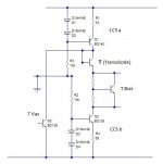
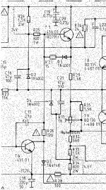
I should see the whole schematic, but I can guess that there is some condition, possibly a shorted output, where the BS capacitor might become reverse biased, and these diodes will prevent that. This is not common. It is common for unnecessary parts to be left in an amp design because the designer never bothered to prove they were required.Steveu,
Can you explain this configuration of parallel diode to capacitor in double bootstrap? (C16//D2 and C21//D4).
- Home
- Amplifiers
- Solid State
- Why bootstrap?