AKSA said:Yes, a bootstrap is more stable at high frequencies.
The reason is one of the paradoxes of electronics, as positive feedback normally makes an amplifier less stable.......
With increasing frequency, and typically starting about 100KHz, the ESR of the bootstrap cap, being electrolytic, begins to rise. A large contribution to this is the self inductance of the foil of the cap; by Xl = 2pifL this steadily rises. As frequency rises further this higher ESR prevents ready charge flow to and from the cap, and by around 300KHz the capacitor has electrically 'shrunk' to a small portion of it's nominal capacitance.
This in turn begins to load up the collector of the VAS as the resistance to rail steadily diminishes. This pulls back gain.
In any voltage amplifier, we have poles, which define the point on the spectrum where negative feedback turns positive. In a global feedback loop we must bring OLG below unity by this pole frequency so that when feedback turns positive, gain is below one and it will NOT oscillate. This is normally implemented with a simple capacitor between collector and base of the VAS.
The bootstrap helps considerably in culling the gain to below unity by the pole frequency. This is a great strength because it means that there is no longer just the one 6dB/octave mechanism, lag compensation, for meeting the Bode-Nyquist criteria.
Cheers,
Hugh
Hello
"The bootstrap helps considerably in culling the gain to below unity by the pole frequency"
So wen I'm use to put a 33 nf capacitor across the bootstrap capacitor of all amps I do, to reduce the total ESR of the bootstrap capacitor, it's not a very good thing to do ?
And maby it's even better to use a big bootstrap capacitor since it's high ESR help to use a smaller cdom capacitor ?
Thank
Bye
Gaetan
Take an amplifier that uses bootstrapp and calculate a CCS to put into the place
Or the opposite, of course...even other kind of circuit can be switched on and off..also can be replaced using switches or relays.
If you need i can do that for you and send by direct mail... the equivalent bootstrapp or equivalent CCS..the substitutor.
Them install, point to point... and a switch to enter bootstrapp or CCS and listen
This is the better way to check things and to evaluate things.
Do it real world and LISTEN.
Why to use Neuroniuns to that..also neuroniuns will never be sure without listening... save your brain for better things..this is something you can conclude using ears and only a small part of your brain, the part responsable to listen things.
regards,
Carlos
Double bootstrapp
Hi all.
Steven said of PL400:
I think the main reason for connecting C11 to the emitter of the driver is that this emitter voltage follows the AC signal on the collector of Q5 much better than the output does, so the voltage across R18 is kept more constant and the collector impedance of Q5 becomes higher and more linear. I think even harmonic distortion is lower because the half wave rectified (class B) non linearity of the voltage across emitter resistors R40, 43, 45 is not fed back.
My questions: the explanation is valid for NAD C-370? Where the botton of double bootstrapp (c14 c15) are connected of the emitter of the drivers - colletors of sziklai output.
And this topology (double bootstrapp in NAD) is valid for EF output?
Thanks
GEirin
Re: NAD C370
Yes, it is a double bootstrap. But here the bootstrap serves a different purpose than in the cases where it creates a high collector impedance for the VAS (for high loop gain). In this case the purpose is to create a constant current source for the emitter followers T15,16, that even works a bit beyond the supply lines to drive the amp closer to the supply lines.
The current through T15, 16 is set by (voltage across the TL431 minus a Vbe) / R38,43.
GEirin said:Hi all.
What is the function of: c14,r45,r46,d11 and c15,r51,r52,d12 network. Double bootstrapp?
Thank
GEirin
Yes, it is a double bootstrap. But here the bootstrap serves a different purpose than in the cases where it creates a high collector impedance for the VAS (for high loop gain). In this case the purpose is to create a constant current source for the emitter followers T15,16, that even works a bit beyond the supply lines to drive the amp closer to the supply lines.
The current through T15, 16 is set by (voltage across the TL431 minus a Vbe) / R38,43.
Hi all
To boot or not to boot, that is the question!
The performance of a bootstrap can certainly be simulated, whatever has been said about sonic performance.
In a simple bootstrap circuit like Linsley-Hood's original Class A, the upper output stage is severely slew-rate limited by the relatively poor fT of the upper output transistor. Bootstrapping is positive feedback, and so if you have a slow output stage, the bootstrap is slow, and the output can only work at the speed of the output transistor as it would be in common emitter mode. So it is quite possible for the input transistor to suffer transient overloading effects- not by a Miller capacitor (as there wasn't one) but because the output stage is slow. The cure for this is to use fast output transistors!
(This maybe why some listeners report that the "sound" of the Class A was not as good as expected. And this would depend on individuals' set-up: what source they used, whether there were hgih frequency content or not and so on. So just because some listeners think that the Class A is fantastic, it may be that their source material is less likely to overload than anothers.)
If you add a driver transistor, the slew rate improves. Becuase the driver usually has a higher fT than the output, it can provide more drive more quickly. So, the response of a driver+output pair will be much better when bootstrapped.
In this case is there any benefit in using a current source, or mirror stage to provide the VAS signal? I suggest the answer to this is yes, because it will improve the slew rate further, making the amplifier sound crisper, perhaps. But this is not a categoric answer because then it all depends ... If you use Miller compensation, this wastes the benefits of a current drive, since it "slows down" the VAS, so although some argue that a CCS is better than a bootstrap, with Miller compensation, it is not clear why.
Of course, if you do not use a Miller, as I have often advocated, then you should be able to spot the improvements in frequency response, but stability is another matter... therefore, it is the amplifier architecture as a whole which needs to be taken into account, not just the bootstrap or not.
Finally, I propose that a balanced driver stage should give lower distortion than a single-ended VAS configuration. In a SE VAS, H2 is prevalent. In a balanced stage, whether fully symmetrical (which seems to me to be OTT - but a current mirror+differential VAS seems worthwhile) at least H2 should be all but eliminated.
So, I would say, if you use Miller, bootstrap or not is less an issue, but without a high frequency driver, bootstrap is "less good".
Cheers
John
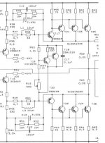
GEirin said:Sorry Steven. Other question.
I´m interested to know the topology the old amplifier attached below.
R9,R10,C7, is bootstrap the VAS TR3?
And R14,R15,C6, is bootstrap a constant current source?
Actually, both bootstraps serve to increase the collector impedance of the VAS. For AC signals both are in parallel; it makes no difference whether the load is connected to the positive supply voltage or the negative supply voltage. The top bootstrap acts as a current source, the bottom one as a current sink. The Vbe multiplier Tr4 is an AC-short circuit between these.
In many (most) amplifiers the VAS (Tr3) is the current sink itself and the bottom bootstrap is not present, i.e. point B of the Vbe multiplier is connected to the collector of Tr3.
In this topology with the double bootstrap the maximum negative output voltage is slightly increased because point B can exceed the negative supply voltage.
Steven
Hi Steven
Thank you very much for your detailed explanations.
You said:
In this topology with the double bootstrap the maximum negative output voltage is slightly increased because point B can exceed the negative supply voltage.
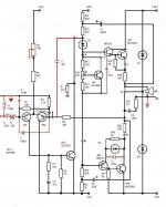
I can to use one diode + R // bootstrap network? Similar to Yamaha circuit attached below?
Guillermo
Thank you very much for your detailed explanations.
You said:
In this topology with the double bootstrap the maximum negative output voltage is slightly increased because point B can exceed the negative supply voltage.
I can to use one diode + R // bootstrap network? Similar to Yamaha circuit attached below?
Guillermo
Attachments
This amplifier probably uses a PNP VAS connected to the positive rail, following the red dotted line. The bootstrap is then the normal load (pseudo constant current sink) for the VAS, including the capability to drive the base of Q220A below the negative supply.
In normal operation D207 is reverse biased and does nothing. Probably it is there for switch on/off protection or overload recovery.
Steven
In normal operation D207 is reverse biased and does nothing. Probably it is there for switch on/off protection or overload recovery.
Steven
Hi Paul
Connect the collector of the VAS (Q7) to the junction of resistor R11 and R12/BD139 collector (disconnecting from R22 and BD139 emitter). Add the second bootstrap resistors to - rail and BD139 emitter, also still connected to R22.
Unfortunately the upper bootstrap now needs to have half the original values as the current has to double. The new bootstrap can use the resistors R8 and R11 you remove, and C9 connected from centre rail to bootstrap point. Add a new bootstrap capacitor (470uF) to the new R8 and R11 values (680 ohms, 1k for example).
This type of double bootstrap was already published by Mullards but they also added a diode in series with the bias transistor (i.e. between R11/VAS collector and R12/BD139c) for reverse bias protection of Q3.
John
Hi Paul
Connect the collector of the VAS (Q7) to the junction of resistor R11 and R12/BD139 collector (disconnecting from R22 and BD139 emitter). Add the second bootstrap resistors to - rail and BD139 emitter, also still connected to R22.
Unfortunately the upper bootstrap now needs to have half the original values as the current has to double. The new bootstrap can use the resistors R8 and R11 you remove, and C9 connected from centre rail to bootstrap point. Add a new bootstrap capacitor (470uF) to the new R8 and R11 values (680 ohms, 1k for example).
John
Hi
I can't understand some of your explanations, can you you use my asc file to draw you circuit ?
I include my asc file.
Thanx
Paul
Attachments
Hi Paul
Connect the collector of the VAS (Q7) to the junction of resistor R11 and R12/BD139 collector (disconnecting from R22 and BD139 emitter). Add the second bootstrap resistors to - rail and BD139 emitter, also still connected to R22.
Unfortunately the upper bootstrap now needs to have half the original values as the current has to double. The new bootstrap can use the resistors R8 and R11 you remove, and C9 connected from centre rail to bootstrap point. Add a new bootstrap capacitor (470uF) to the new R8 and R11 values (680 ohms, 1k for example).
This type of double bootstrap was already published by Mullards but they also added a diode in series with the bias transistor (i.e. between R11/VAS collector and R12/BD139c) for reverse bias protection of Q3.
John
I had modified the .asc file posted in the other thread by tessier as per your instructions above. Is it OK now? Can you kindly correct the Diode position?
--gannaji
Attachments
Last edited:
Hi
Your second file is right.
THe purpose is twofold. First, in the event of a short circuit, it protects the npn driver from being reverse biased beyond the breakdown limit. Secondly it protects the VAS from excessive current flow since the current will be limited by the upper bootstrap resistors. Though the dissipation in these will be higher, so it is advisable to use higher power resistors in these positions (e.g 2W).
John
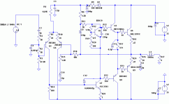
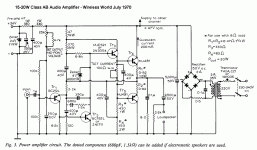
Triple (?) Bootstrap of JLH
Dear John,
Thank you for your kind reply.
In the 15-20 Class AB amp, picture below, the original article in Class A site, (The Class-A Amplifier Site - JLH Class-AB Amplifier) JLLH mentions that
" The first two transistor voltage amplifier stages of this follow conventional design practice, with the collector load resistor of Tr2 boot-strapped to obtain large voltage swing at the base of Tr3 with as little second harmonic distortion as practicable. The collector of Tr3 is also partially boot-strapped in order to reduce the peak voltage swing, and improve the symmetry of the output waveform prior to the application of the loop negative feedback. (Without overall n.f.b. the distortion at full output power is a little less than 4%, almost entirely second harmonic. This is similar to the performance of a good triode valve output stage prior to the application of n.f.b.) The lower end of R3 is also fed with the output signal to improve the output voltage swing obtainable from Tr5."
What are the advantages / disadvantages of JLH method compared to the one above? Can you kindly elaborate for my education only.
--gannaji
Attachments
Last edited:
- Home
- Amplifiers
- Solid State
- Why bootstrap?