Running into a problem - maybe you can assist. I have replaced the LTP on both boards, matched using a Chinese-made tester (average of 4-5 tests) and installed the closest matches, but the offset remained at 90mV and never goes below 75mV on either channel.
Then I disconnected each channel and checked the current draw on +/- of each channel. the Left channel worked fine, set the current at 800mA (800mV across a 1r 10w resistor on each rail) Then I get to the right channel and the positive rail is drawing about 300mA of additional current and fluctuates up and down by ~100mV (measuring 1.0V on the positive and only 750mV on the Negative rail)
So it's been about two weeks and today I tore apart the Right channel and replaced the remaining ZTX657/757s on the input board, checked all the outputs again (they all check good), reinstalled and the negative bias' fine to 800mA, but the right channel is 1.1-1.2mA and fluctuates ~100mA.
While I was replacing the transistors I pulled the 25k pot and checked it, seemed to work fine using a DMM to measure +/- adjustments.
Right channel still has ~55mV of offset even after all the changes.
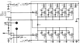
Any thoughts why I would have larger draw on the positive rail, only on the right channel? I measured at the outputs and they all have almost identical voltage on the pins of the Lateral mosfets. This B2 version (4 pair outputs/channel) does not have any source resistors, but all the outputs are heating evenly and with a thermometer they are all show the same temp. as well as the super-scientific "finger" test.
Then I disconnected each channel and checked the current draw on +/- of each channel. the Left channel worked fine, set the current at 800mA (800mV across a 1r 10w resistor on each rail) Then I get to the right channel and the positive rail is drawing about 300mA of additional current and fluctuates up and down by ~100mV (measuring 1.0V on the positive and only 750mV on the Negative rail)
So it's been about two weeks and today I tore apart the Right channel and replaced the remaining ZTX657/757s on the input board, checked all the outputs again (they all check good), reinstalled and the negative bias' fine to 800mA, but the right channel is 1.1-1.2mA and fluctuates ~100mA.
While I was replacing the transistors I pulled the 25k pot and checked it, seemed to work fine using a DMM to measure +/- adjustments.
Right channel still has ~55mV of offset even after all the changes.
Any thoughts why I would have larger draw on the positive rail, only on the right channel? I measured at the outputs and they all have almost identical voltage on the pins of the Lateral mosfets. This B2 version (4 pair outputs/channel) does not have any source resistors, but all the outputs are heating evenly and with a thermometer they are all show the same temp. as well as the super-scientific "finger" test.
If you're using the single ended inputs then I'd say the offset you're seeing is normal. I had the same issue. I ultra matched a set of LTP transistors. Normally when I do this I'll get low single digit offset measurements (like 1 - 2mV) in any amp LTP I put them into, but not the White amp. However when I connected the amp up using the XLR inputs the offset would drop to < 10mV but using the RCA inputs it was quite high. This was the case both on my Audio Precision system and with my Adcom GFP-750 preamp.
As far as your out of balance current draws. I'd say that if you have one channel with a high imbalance between the positive and negative rails then IMO it would imply a bad output(s) mosfet in that channel. If the offset is reasonably low in that channel, then you have to ask where is that additional current going because if it were going to the load then you should have a high DC offset? One thing that comes to mind, where are you measuring the current draw for the channels, is it between the respective channel rectifiers and the main caps or between the main caps and the channel module itself. If the former then the extra current draw could be due to a bad main PS cap, if the latter then it implies a failure in the channel module sinking extra current to ground and not the load. You may want to recheck the insulators on the output mosfets in the affected channel.
Maybe someone else will chime in with their opinion, but this seems like the most likely possibility to me. You could temporaily swap the predriver boards from channel to channel if you think the issue might be there, but I do not see this being the case.
Thanks for the insights... so I tore it back apart and added (16) 0.47r 2w source resistors on both channels (prefer 0.22r, but didn't have any on hand). Reset the bias on both channels at 800mA per channel (used a 1r 10W resistor between bridge rectifier and supply capacitors. Still has about 0.250mV turn on thump and about -1.20mV turn off thump but otherwise appears working/heating as it should.
Current state (using RCA inputs):
Right channel is now down to 15-20mV (this channel has all new matched to-92s on the input board)
Left channel remains at 75-85mV (this channel has new matched TO-92s for Q1, Q2 and Q3) - so changing them and adding source resistors did nothing.
Listening for about 3-4 hours and sounds good, with a slight concern about the 80mV on 6.4r speaker (~12.5mA, or ~10mA more than Right channel)
Last edited:
Some observations/hints:
Resistors added at the source pins will address current sharing among the output FETs but, since they are inside the feedback loop, there's unlikely to be any detectable change in output offset behavior.
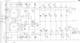
This amp doesn't have any input blocking cap, so be sure to measure DC voltage from signal source at the amp input, from Q1 base to GND1. In principle, any DC present at input will add with unity gain to the output. A blocking cap might be a good idea.
Remember output offset arises from Vbe mismatch, and bias current drops across bias resistors. Measure input bias currents by measuring drops across R5 and R12. Ideally, they will be equal. Swapping Q1 and Q2 and noting change can be insightful.
Be alert to possible leakage current in C1; just 1uA of leakage will add 10mV to output offset. [If C1 is suspicious, you can sub a low leakage 1uF film cap as diagnostic test. Low cutoff frequency will be inadequate, but the cap will keep the amp stable during bias check.]
Resistors added at the source pins will address current sharing among the output FETs but, since they are inside the feedback loop, there's unlikely to be any detectable change in output offset behavior.
This amp doesn't have any input blocking cap, so be sure to measure DC voltage from signal source at the amp input, from Q1 base to GND1. In principle, any DC present at input will add with unity gain to the output. A blocking cap might be a good idea.
Remember output offset arises from Vbe mismatch, and bias current drops across bias resistors. Measure input bias currents by measuring drops across R5 and R12. Ideally, they will be equal. Swapping Q1 and Q2 and noting change can be insightful.
Be alert to possible leakage current in C1; just 1uA of leakage will add 10mV to output offset. [If C1 is suspicious, you can sub a low leakage 1uF film cap as diagnostic test. Low cutoff frequency will be inadequate, but the cap will keep the amp stable during bias check.]
@BSST still digesting a lot of what's in your post and suggestions - but appreciate you taking time to add ideas and an explanation of how the parts in the circuit work - still learning as I go.
1) Measured the RCAs from the Pre powered on, no music playing and I get 0mV of DC on right and left cables
2) Measured across R5 input connected to Pre, no music playing (47mV on Left, 46mV on Right)
3) Measured across R12 input connected to Pre, no music playing (120mV on Left, 115.5mV on Right)
4) C1 is brand new Nichicon 35V 220uF - UKW (black foil/gold writing and not specifically a low leakage Cap like UKL)
Maybe that's my issue, because the datasheet does specify it has 77 to 231uA of leakage current, where the UKL specs at a maximum of 15.4uA?
Another finding, is that the right channel starts out at 15mV offset, but once the amp is fully warmed up (1-2 hours of music) it is back at ~60mV, where the left channel stays at 75-80mV the entire time (cold to warm)
I'm not looking for 0mV offset - but close to 25mV would make me feel better using the amp with my different speakers.
edited - added part about RCA DC from Pre
Try measuring the DCV drop across R11. I think there could be on the order of 0.7mV present, enough to explain much of the offset error.
I should have ask you to report some voltage readings as signed numbers re ground. So I believe Q1 base voltages are about -46mV and I think output offset is +75mV. And would you also report Q2 base voltage re GND1?
Thanks!
I should have ask you to report some voltage readings as signed numbers re ground. So I believe Q1 base voltages are about -46mV and I think output offset is +75mV. And would you also report Q2 base voltage re GND1?
Thanks!
Last edited:
I will need to tear it down to get at these spot to measure, very close quarters all put together.
I quickly did my best to measure R11 - 0-1mV across it on both channels
I will come back with the other readings
I quickly did my best to measure R11 - 0-1mV across it on both channels
I will come back with the other readings
Update - I could not figure out how I kept getting high offset and unbalanced bias current (using 1r 10w resistor in line between caps and amp boards)
Issue(s) - high offset 55-70mV on both channels and went up with a source plugged in.
Also, right channel had 900mA on the positive rail and only 650mA on the negative over a 1r resistor. I changed all small signal transistors and measured every resistor and diode.
I was about to give up and did a final search on lateral mosfet schematics and found none with a 33pF cap from rail to Gate on any production amp except this White Audio. So what do you do but despiser one leg off the mosfet and bend it out of the way. What happened - <5mV offset on both channels now, this is down from 55-70mV and would go up to >100mV with the inputs shorted or connected to a source (tried CD, MP3, iPhone and HT pre-amp and they all have high offset)
So all is well that end well - I have biased to 120mA per mosfet across the 0.47r source resistors I added and the amp powers on, idles up nicely and plays music.
Still need to test how it behaves with a decent speaker but want to test fully before I trust it with something of quality.
I’ll let you know my listening impressions in a few days.
Thanks to @Chamberman for posting schematics, very helpful in my troubleshooting journey.
Great job! Your perseverance has been rewarded!
So your amp had gate-drain 33pF caps tacked in? At each of the each of the 12 output FETs?
Do you think the amp may have been oscillating and removing the caps cured?
Thanks. And again congrats.
So your amp had gate-drain 33pF caps tacked in? At each of the each of the 12 output FETs?
Do you think the amp may have been oscillating and removing the caps cured?
Thanks. And again congrats.
Yes exactly - gate/source 39pF caps (CGO), my amp has 4-or outputs not 5-or like the OP. Otherwise identical design.
I assume it was oscillating but only causing bias fluctuations on the right channel, otherwise DC offset issue on both channels.
Weird symptoms and can only assume that these caps were added when the previous owner had the amp re-capped and possibly why he sold it (hum, hiss and distortion complaints).
I doubt there would be any benefit either way. So it's likely you have a known good cap for future work. 😉
I want to review all the posts to see if I overlooked a clue. If you were seeing varying offset associated with changes in source impedance (assuming DC block in the input), that's a good reason to suspect oscillation. I should have been alert to oscillation as possible culprit, but wasn't.
I want to review all the posts to see if I overlooked a clue. If you were seeing varying offset associated with changes in source impedance (assuming DC block in the input), that's a good reason to suspect oscillation. I should have been alert to oscillation as possible culprit, but wasn't.
I was about to give up and did a final search on lateral mosfet schematics and found none with a 33pF cap from rail to Gate on any production amp except this White Audio. So what do you do but despiser one leg off the mosfet and bend it out of the way. What happened - <5mV offset on both channels now, this is down from 55-70mV and would go up to >100mV with the inputs shorted or connected to a source (tried CD, MP3, iPhone and HT pre-amp and they all have high offset)
Well that's interesting especially given the fact that the amp I was working on had no capacitors. There are some production designs that used rail to gate caps. The Borbely audio Servo amps used them but only on the positive rail, see attached picture, they were 39pF. Also the later Hafler Transnova 9300/9500 amps used a single 22pF from rail to gate. Did you happen to test the caps that were pulled? I'm wondering if one of them had failed.
At any rate, I'm glad you got it sorted out.
Attachments
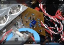
I mis-spoke earlier - the caps are 39pF and go from Pin 1 (on output) to Pin 3 (on board) on the N-channel (k1058) side of the outputs, so Gate to Drain. I did have a couple that broke in half when I was untacking them from the outputs, but unsure if that was me being careless with the soldering iron, or they were in fact already broken. They are very small COGs likely not more than 100V, so highly possible I melted them with a careless touch.
I originally replaced the two that fell apart on the right channel, replaced all of them with 22pF and 200V parts I have on hand so they would all match. There was no change, so I opted to unsolder one leg (Gate) and leave attached to the Drain part of the board. Easy enough to replicate on the Left channel because those 1058 outputs are on the top of the heatsink (right channel they are on the bottom), so I could do it without taking anything apart.
I have listened and enjoyed it for the last few days - but still have some odd behavior (assume it's the schematic/design). Both channels have much lower DC now without any input connected (35mV on left, 15mV on right). However, when I plug in a source, or short the inputs the DC goes up, ~70mV on left and ~50mV on right channel.
Not complaining, it's much better than it was - just can't understand why? The pre-amp circuit seems basic and has compensation to be stable.
Any idea if there is an easy way to add a pot between/after the input pair to null the DC? Does it really matter (better??) if I could null it using a pot with inputs shorted, so it goes negative without a source connected? Modifying the circuit is a little over my head, especially adding components and making sure they don't cause more harm than good.
I would compare open circuit offset with offset when inputs are shorted via 0.1 uF caps. If different readings, I would be concerned about possible oscillation. Also, look carefully for any DC presented from source that may contribute.
I don't recall if you have scope to look for oscillation.
I don't recall if you have scope to look for oscillation.
For offset adjustment a simple offset trimmer can be added using a resistive divider between the DC rails and a pair of diodes to limit the adjustable voltage. See the attached schematic of the Aragon 4004 which uses this type of simple offset adjustment. R28, R29, D1, D2, R24, and RV2 are the components you'd need to add.
However the offset would have to be much higher, well above 100mV, before I'd consider doing this. If you put your amp on an analyzer you'll not measure any more distortion with 70mV than you do with 5mV.
However the offset would have to be much higher, well above 100mV, before I'd consider doing this. If you put your amp on an analyzer you'll not measure any more distortion with 70mV than you do with 5mV.
Attachments

Yeah, agree that it doesn't really make sense and won't make a difference to the performance. I will enjoy as it sits. Thanks again for posting schematics and jumping in with help and assistance.
Hi, All.
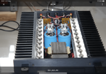
Thank you for posting and sharing the issues and resolutions regarding to the White Audiolab amp. I happen to own a 250wpc White Audiolab power amp. Overall performance sound wise I think it does OK. But looking inside ,IMO, it is abit with DIY look indeed. But love its simplicity though.
Yootk.
Thank you for posting and sharing the issues and resolutions regarding to the White Audiolab amp. I happen to own a 250wpc White Audiolab power amp. Overall performance sound wise I think it does OK. But looking inside ,IMO, it is abit with DIY look indeed. But love its simplicity though.
Yootk.
Attachments

- Home
- Amplifiers
- Solid State
- White Audio Labs B3 amplifier rebuild (Schematic included)