Exellent, so I can just lose R5 and it will work ok? Thanks. 🙂jethdub said:I believe that as you are using TL072 amps the resistor on the non-inverting input isn't necessary as Dc offset is not such an issue with FET input amps.
EDIT: Would it be worth adding input buffers before the voltage summer?
As long as both inputs are being driven by like sources, as in output impedance, there's probably little need to buffer them.
🙂
🙂
Hi,MikeHunt79 said:
http://users.cscs.wmin.ac.uk/~wooda/components/opamps/
Now, the part which concerns me is "R5 should be parallel combination of R1-4 (R1-3 including source impedances)."
I'm not really sure what the source impedance is, but would using input buffer solve this? Or could I just get rid of R5 and have an inverting summer?
the non-inverting input needs a resistor to ground on the input to supply the matching input offset current that the FET opamp expects to see.
This offset current is very small and the opamp will tolerate a significant error in the matching and still give an output with acceptable output offset.
But, the solution is easy.
Add A DC blocking capacitor to the input and take the resistor to ground. This way the filters and opamps are protected from DC coming from the source and the input offset current is supplied by the signal ground connection.
I recommend the inverting opamp as a summer. But remember the gain is defined by the value of all the parallel input resistors and their source resistances.
jethdub said:
Juma, I notice on your schematic that you have seperate PS and signal grounds marked. Are these grounds just seprated on the board but fed from a single cable to the star or central grounding point, or are they seperated all the way back to star ground?
Is it normal practice for you to seprate your grounds or only for certain circuits?
This is something I've been reading on recently and it doesn't seem to be at all straightforward so I'd be interested in hearing about your approach. Thanks.
Hi Jet,
if you look at the bottom view pic you can clearly see the ground arrangement (black wire is power gnd). It's a bus ground scheme that leads to amps' star ground point with 10 Ohms loop-breaker. You can see many good examples in Pass Labs forum and passdiy.com (http://www.passdiy.com/pdf/zen-v4.pdf for instance)
Yep, they are all from the same source... 4 channel headunit. 🙂 I'll skip the input buffers then.poobah said:As long as both inputs are being driven by like sources, as in output impedance, there's probably little need to buffer them.
🙂
Yep, I've used 10k resistors so the sum of both voltages should go to the output, without the output voltage being multiplied or divided...AndrewT said:
Hi,
the non-inverting input needs a resistor to ground on the input to supply the matching input offset current that the FET opamp expects to see.
This offset current is very small and the opamp will tolerate a significant error in the matching and still give an output with acceptable output offset.
But, the solution is easy.
Add A DC blocking capacitor to the input and take the resistor to ground. This way the filters and opamps are protected from DC coming from the source and the input offset current is supplied by the signal ground connection.
I recommend the inverting opamp as a summer. But remember the gain is defined by the value of all the parallel input resistors and their source resistances.
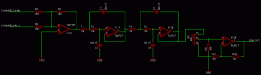
Ok, so If I have a 100nF cap between the signal and ground on both channels 3 & 4 before they reach the summer resistors, that should get rid of the DC offset problem?
I'm not quite sure what you mean tho when you say "take the resistor to ground"... do you mean I should have R7/R8 inline with the 100nF cap between sugnal and ground (instead of it being in-line with the signal)?
Ooops, I've changed it to a 7915 now, thanks. 🙂juma said:Mike, your schematic from post #17 won't work: IC2 should be 7915 (negative voltage regulator)
Finally, for the output buffer, I looked high and low and couldn't find a 20k pot. Could I use a 10k pot if I changed all the fixed resistors in the output buffer (r9,r10,r11) to 5k?
Mike,
go back and look at the opamps link you posted.
initially I'll use the last three diagrams for explanation.
Take the last one. High pass non-inverting unity gain S&K 2pole filter.
The first capacitor acts as the DC block and ensures that any DC present in the input signal does not pass to the output of the filter.
The two diagrams above show the input resistively coupled to the opamp input pin.
These two, the summer and the low pass, will send DC in the input signal to the output.
They both require a high pass filter (=DC block) on the signal line.
A series capacitor that is big enough to pass ALL audio signal can be inserted between source and the diagrams. Somewhere around 1uF to 10uF should be about right for most filter circuits and buffers. A low impedance buffer may require the series C to be as high as 100uF (Rane, as an example, suggest 220uF for their balanced lines). The resulting diagram will look like the AC coupled amplifier but without the biasing and C2 on the non-inverting pin.
Now the summer. If r1=r2=r4 (for a two channel summer) then the gain for each channel is 0db (=1times). If the signal on the two inputs is identical in voltage AND phase then the output is twice the single input voltage i.e. output voltage =V1+V2. This is due to the two input summing resistors being in parallel and presenting a net source resistance of 5k (=10k//10k) the gain becomes 10k/5k (R4/Rsource) = +6db (2times).
Now the resistor to ground ambiguity.
The high pass filter is a capacitor in series with the signal and the Resistor takes the output of the capacitor to ground. The feed to the next stage is taken from the junction of the C&R.
Look at non inverting amplifier (diagram4). R3 is the resistance seen by the non-inverting input pin and the formula says that this resistance should be the parallel sum of the two resistors attached to the inverting pin. For a gain of 2, both these resistors, R1=R2=10K, have a parallel sum of 5k. The formula says that R3=R1//R2=5k.
If you fit a DC blocking cap in front of this resistor then the effective resistance seen by the non-inverting pin is infinity due to the perfect capacitor. Instead what we can do is take the resistor from input pin to ground and take a second feed from the non-inverting pin to the DC blocking cap and then to the signal input terminal. The opamp still sees 5k resistance AND the signal has a DC blocking cap in it's route.
Just wanted to check something that I realised I ws unsure of looking at Mikes schemos. The first filter stage is fed from the summing amp, is the source impedance then the 10k summer feedback resistor in parallel with the opamp output?
Yes, the pair of impedances add in parallel.jethdub said:The first filter stage is fed from the summing amp, is the source impedance then the 10k summer feedback resistor in parallel with the opamp output?
The 10k feedback resistor is usually ignored due to the low value of opamp output impedance. This Zout is probably <10r and may be a lot lower.
Thanks, I knew that really, just that whilst on the learning curve and with so much information to absorb at times things become a little confused...
This has been on the back burner for a while, but I haven't forgot about it...
I'm about to order the parts now, and I've already got loads of metal film resistors, but I haven't a clue what sort of caps to get...
All I know is that electrolytic ones can't be used, as they are not bipolar... so what caps would be best out of these?
Aluminium Electrolytic (7,290)
Carbon Aerogel Foam (67)
Ceramic Disc & Plate (1,432)
Ceramic Multi-layer (9,275)
PET (96)
Paper (60)
Polycarbonate (14)
Polyester (1,821)
Polyphenylene Sulphide (331)
Polypropylene (1,533)
Polystyrene (144)
Related Products (4,048)
Silvered Mica (216)
Tantalum Electrolytic (4,298)
Low cost op-amp alternatives:
- NE5532 is great for driving long signal lines or low impedances. It has a low input impedance so it's not recommended for filters.
- LM833/LM837 are good overall, except in high impedance filter circuits.
- TL07x is good for high impedance filters due to the FET inputs resulting huge input impedance.
MikeHunt79 said:so what caps would be best out of these?
Ceramic Multi-layer - C0G or NP0 types only
Polyester
Polypropylene
Polystyrene
and if you can still obtain them add polycarbonate to the list.BWRX said:
Ceramic Multi-layer - C0G or NP0 types only
Polyester
Polypropylene
Polystyrene
Thanks guys, I've gone for some ceramic ones.
Eva, I've gone for TL072's, by the looks of it they should work. 🙂
Eva, I've gone for TL072's, by the looks of it they should work. 🙂
- Status
- Not open for further replies.
- Home
- Amplifiers
- Chip Amps
- What op amps are good for this crossover circuit?