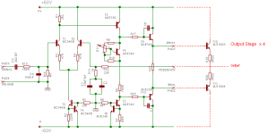
Hello all!
At the moment I'm trying to design my first amp.
Although I'm a bit experienced in electronics design (especially digital and microcontroller), I've no experience in amplifier design.
Please tell me your impressions about the
attached schematic!
Some parts have no value yet because this is only the first draft.
Thanks!!
Patrick
Attachments
Hello Patrick
Your design is very good, I just suggest minor changes :
Differential input amplifier must be dc balanced : R14 must be same value as R12, 22 k. And R1 must be adjusted so that the dc current in T1 and T2 is the same (1.5 mA).
Before this adjustement, it can be a good idea to insert a small resistor in the emitter of T5, I suggest 68 ohms, in order to improve the linearity of this stage.
C4 seems to be very high, 1 nF is sufficient.
BC546B offers poor security margin with Vce limit, I suggest 2N5551 or equiv, for T1, T2 and T3. If you experience some noise problems with the input stage, the right ansver is to design a cascode configuration, with BC546B *and* 2N5551
It may be necessary to connect a small capacitor across R12 (100 pf...), and a resistor in series in the base of T2 (same as R15).
>>> If your amp is biased in AB class :
Great care must be taken to adjust the idle current, in order to minimize crossover distorsion. You can connect a capacitor (1 uF, film) across R13, between the bases of MJ15003 and MJ15004, to speed up the commutation of this transistors, reducing high frequency crossover distortion (this because MJ15003/4 are slow devices, only 2 MHz ft)
A problem can occur with C6 and C5, I suggest to remove this capacitors and replace them by one between base and collector of T5, this is a more usual arrangement, which cannot disturb the commutation of final stages at high frequencies.
Finally, it can be useful to insert some decoupling in the power supply rails, between T5-T9 and T7-T10, in order to insure a clean operation of the input stages, in despite of the transients induced in wires inductance by the final stages (Glitches ? Correct word ?)
Regards, P.Lacombe.
Pardon me, I have forgotten this (output stage x4...)
MJE340/350 exhibit significative gain loss beyond 150 mA, and cannot be used as drivers ( T9 and T10) Motorola has developped specially MJE15030 and 15031 for this purpose. They work wery fine.
Regards, P.Lacombe.
MJE340/350 exhibit significative gain loss beyond 150 mA, and cannot be used as drivers ( T9 and T10) Motorola has developped specially MJE15030 and 15031 for this purpose. They work wery fine.
Regards, P.Lacombe.
Amplifier design
Mr. Lacombe is hereby certified as an experienced amplifier designer. Great suggestions. Please post some more.
H.H.
Mr. Lacombe is hereby certified as an experienced amplifier designer. Great suggestions. Please post some more.
H.H.
Hi,
As usual, when the MJ15003/4 get into the discussion, there is an alternative in MJ21193/4 instead.
They stand the work better and you could probably go for 2xoutput stages instead of 4 (= cheaper + less holes to drill).
It looks like you are going for some 200+ Watts into 8 ohms. Some good references to look for help is to be found at:
http://users.ece.gatech.edu/~mleach/lowtim/
and
http://sound.westhost.com/project3a.htm
If you don't want to go with the BC546's you could use MPSA06, because if you go with the MJE15030/31, then you have only Motorola/On Semiconductor devices, which could be an advantage when you get your parts.
Make sure that T8 keeps the same temperature as the output devices (T11/T12). Othervise you'll get some drifting in your biasing. In the Leach Amp this is solved by adding a bunch of diodes glued to the heatsink in series with/instead of your R9.
Good luck!
//magnus
After some meditation, it becomes evident for me that it is one another problem with the design. The voltage gain of the second stage T5 is not well definite, because he is loaded only by the input impedance of the drivers T9 and T10, which is very dependant of many things such frequency, amplitude, etc. of the signal.
Its seems necessary to connect a resistor between the collector of T5 and the ground, and one another in the same manner for T7. I think that 6.8k is a correct, but the current of T5/T7 will be insufficient, it is necessary to reduce R7 to 33 ohms. The resistor added in the emitter of T5 is also to be modified.
Regards, P.Lacombe
Power Amp Schematic
Hi Patrick,
If you have a look at the schematic of the Son of Ampzilla
http://home.earthlink.net/~narf1/sonamp.jpg
which is 25 years old you will note the similarity with your scheme. The Son has full complementary circuitry giving twice the drive to the output transistors. Any reason you choose not to use complementary circuitry?
MJ15003 and 04 seem to be a bit slow for audio. I am using now in my Ampzilla MJ21193 and MJ21194 sucessfully.🙂
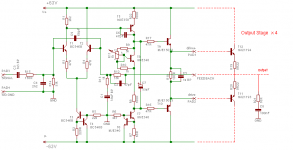
2nd revision
Hi,
thank you all for your suggestions!
Here is the 2nd revision with some changes.
I used MPSA06 instead of the BC546B in the LTP and the current sink.
Further I used the MJ15032/33 because I didn't find models for the 30/31.
In the output stage I used 4 pairs MJ21193/94.
When simultating this design I see approx. 180mV offset voltage at the output which seems a bit high, isn't it?
Further I found that I may have to use a darlington as T5.
The amp is biased to work in Class AB.
My friend (for whom this amp is) has some very high quality speakers and therefore I thought about biasing it for a idle dissipation of about 100W with maybe 8 pairs of output devices. With the right heatsink of cause. What do you think?
After looking at the schematic in Mr. Kwak's post:
What is the advantage of using 2 differential pairs? Only the gain?
Attachments
Hi,
I don't want to be a stick in your butt, but hooking a pair of really expensive speakers to your first homebuilt, home designed amp... That's scary... I've fried a couple of speakers with my Leach Amp before I got it running perfect.
You better build a DC protection circuit as well before you try it on your friend's speakers!
Good luck!
//magnus
Hello swede,
I'm REALLY not planning to use his speakers as the first, 2nd or third test speakers.
I should have said that I only plan to connect these speakers when the amp is running perfectly.
The amp will have DC and temperature protection maybe clipping too (not indicator, protection! ).
Patrick
I'm REALLY not planning to use his speakers as the first, 2nd or third test speakers.
I should have said that I only plan to connect these speakers when the amp is running perfectly.
The amp will have DC and temperature protection maybe clipping too (not indicator, protection! ).
Patrick
P.Lacombe did write : "Differential input amplifier must be dc balanced : R14 must be same value as R12, 22 k. And R1 must be adjusted so that the dc current in T1 and T2 is the same (1.5 mA).
Before this adjustement, it can be a good idea to insert a small resistor in the emitter of T5, I suggest 68 ohms, in order to improve the linearity of this stage."
You have added a emitterresistor on T5, but T1 and T2 can still be in inbalance. Try measure Ic on T1 and T2 in your simulation.
Try raise or lower R1 and observe your offset voltage.
Thats why some people add a currentmirror instead of R1. It is easier to get DC current balance.
Sonny
If you use two complementary diff pairs you should be able to cancel out input bias currents wich normally would flow through your feedback resistors. These bias current will flow between the bases of the npn and pnp transistor.
But this is theory because then you would need npn and pnp pair with same currentgains. In real life it will remove some of the inputbias currents but not all.
If you use JFET's instead you "only" have to deal with offsetvoltage.
Compared with your amp with a single diff pair and a current sink in the second stage i would say that a complementary pair will ~double your gain.
Sonny
Hi P.Lacombe
"MJE340/350 exhibit significative gain loss beyond 150 mA, and cannot be used as drivers "
I dont really understand, where is this current lost? Is it just when you have alot of transistors in the output stage that it becomes a problem or should I also change the 340/350 in my design when I only have 2 transistors in the output stage? I guess it cant hurt.
Jonas
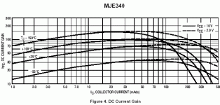
JKLman: If you look at figure 4 at:
http://www.onsemi.com/pub/Collateral/MJE340-D.PDF
You'll se that the current gain drops at about 150 - 300 mA.
//magnus
http://www.onsemi.com/pub/Collateral/MJE340-D.PDF
You'll se that the current gain drops at about 150 - 300 mA.
//magnus
Attachments

For 100watts only, i don't think you need that much of output devices. I think you should riase the power since you are using 63 volts. I built the ROd's 3A project using 42 volts and it will give out 90 watts with only one complimentary pair with the Iq at 100ma. How bout trying Jap transistors if you can find them.
Sc3281 and Sa1302. ft of 30 mhz, higher gain at low to high current compared to the motorolla's. check this out at andrea cuff's site. Just my suggestion.
Sc3281 and Sa1302. ft of 30 mhz, higher gain at low to high current compared to the motorolla's. check this out at andrea cuff's site. Just my suggestion.
Hello NickC,
I did not mean 100W output.
I meant 100W idle dissipation (!)
When you use +-42V and 100mA Iq
then your idle dissipation is 8.4W.
The C3281, A1302 are very nice transistors but I found that they are hard to get at a reasonable price. In germany they cost 14 EURO per pair (not matched of cause). 😱
Patrick
pprasse said:Hello NickC,
The C3281, A1302 are very nice transistors but I found that they are hard to get at a reasonable price. In germany they cost 14 EURO per pair (not matched of cause). 😱
Patrick
no they cost 5 EUR the pair, at least, when you get the best German mailorder dealer for Japanese semiconductors ...
it is Gerwert, phone 07753-92130
BTW, the Toshiba C3281, A1302 have been replaced by new numbers, all specs identical, same package, same price. Go to the Japanese Toshiba semiconductor web site to get data sheet.
regards,
Hartmut
- Status
- Not open for further replies.
- Home
- Amplifiers
- Solid State
- What do you think about this amp schematic?