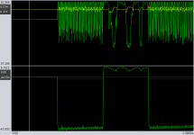
pprasse said:The upper waveform is from the net where you can read LTPout1 in the schematic. (30% from top, center)
The lower is from LTPout2 ( right from LTPout1).
The waveform is 1kHz. (see scale at bottom)
Patrick
Should be okay.Patrick, It depends how hard the VAS stage is loaded. What is you loading of the amplifier and how large is your output signal of the amplifier.
With no load the LTPout1 waveform should be smaller. What is the peak-peak voltage of the waveform.?
If you run a squarewave through the amp the LTPout1 should have spikes which are placed on the rising or falling edge of squarewave it is because of the rapid charge/discharge of miller cap/stray capacitance on the VAS stage. Try it out.
Sonny
Patrick,
In my opinion, implementing a current mirror is not indispensable, because of the constant current in the emitters. You have just to decrease R1 to obtain the same current in T1 and T2, very simple and efficient. As you have seen, the best current mirror cannot have as low distortion as a simple resistor.
"Simplicity, linearity" (Nelson Pass).
Regards, P.Lacombe.
Vpp (LTPout1) = 1.31 V
Loading of the amp is 4R, Vpp (output) = 94V
Vpp (signal) = 1.4V
With no load Vpp(LTPout1) = 0.92 V.
I will simulate squarewave later because when I try to simulate spice eats up all my CPU time.
Therefore I think it "hangs".
Thanks!
Loading of the amp is 4R, Vpp (output) = 94V
Vpp (signal) = 1.4V
With no load Vpp(LTPout1) = 0.92 V.
I will simulate squarewave later because when I try to simulate spice eats up all my CPU time.
Therefore I think it "hangs".
Thanks!
Oh. It didn't hang. It took 500 sec (500MHz CPU, highest priority).
Think this was due to the infintitly short rise and fall time of the square wave.
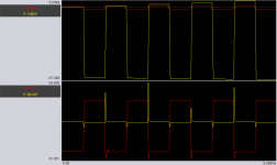
Hmm... The signal doesn't look very nice...
Ok:
upper panel:
yellow: ltpout2
green: ltpout1
lower panel:
red: signal ( 0 - [-1.4V])
green: output
Some nice traces of oscillation, don't you think?
Think this was due to the infintitly short rise and fall time of the square wave.
Hmm... The signal doesn't look very nice...
Ok:
upper panel:
yellow: ltpout2
green: ltpout1
lower panel:
red: signal ( 0 - [-1.4V])
green: output
Some nice traces of oscillation, don't you think?
Attachments
hehehe... yes!!! you are right. mmmhhh what did go wrong. I am ... okay give me a half hour! I will write back.
Sonny
Sonny
What did your sine voltage look like on the output?
Try raise c6 to 1nF .. I know it lowers your bandwidth a lot but.. Try it and run two new sims for sine wave and squarewave.
Sonny
Try raise c6 to 1nF .. I know it lowers your bandwidth a lot but.. Try it and run two new sims for sine wave and squarewave.
Sonny
The sine looked like a sine.
No, seriously: It looked like a very good and smooth sine with approx +10mV offset.
With 100nF the you can see the glitches the spikes perfectly (with square wave),
but the sine is more or less like this:
( I don't know the english word) /\/\/\/\ on the output
No, seriously: It looked like a very good and smooth sine with approx +10mV offset.
With 100nF the you can see the glitches the spikes perfectly (with square wave),
but the sine is more or less like this:
( I don't know the english word) /\/\/\/\ on the output
I cannot tell you right know why it oscillates... I am at work right now, and i don't have the time to simulate this circuit right now.
What i can tell you is that you have a heavy loading of VAS stage. You drives as sink and source +/- 6.5mA (1.31Vpp on the base of T5 ~ same on the emitter) from your VAS stage when driving 4R at 94Vpp.
Personally i would add another buffer between VAS stage and the output stage.
Maybe you should try run some sims first with R1 (1.8k .. 2k7) as suggested by P.Lacombe. Take some look at DC Offset,Gain, phase, Look at sinewave and squarewave signals.
Then later try add the currentmirror and do the mods in order to get it up and running with the currentmirror.
Sonny
pprasse said:The sine looked like a sine.
No, seriously: It looked like a very good and smooth sine with approx +10mV offset.
With 100nF the you can see the glitches the spikes perfectly (with square wave),
but the sine is more or less like this:
( I don't know the english word) /\/\/\/\ on the output
/\/\/\/\ = Triangle
Thanks for your help!
I will do some more tests and write my results
in the evening ( 9-10h GMT).
The DC offset was very small with the sinewave. I think one can go with 10mV?
Triangle, sure. Thanks.
Regards,
Patrick
I will do some more tests and write my results
in the evening ( 9-10h GMT).
The DC offset was very small with the sinewave. I think one can go with 10mV?
Triangle, sure. Thanks.
Regards,
Patrick
transistor subs
Hifidaddy, what are the new subsitutes for the Jap. transistors?
Pprase, how do you go about counting the idle dissipation. (Newbie) . How do you calculate the power of your amp.
Hifidaddy, what are the new subsitutes for the Jap. transistors?
Pprase, how do you go about counting the idle dissipation. (Newbie) . How do you calculate the power of your amp.
NickC,
How to calculate idle dissipation? Well, use Ohm's law. U=R*I, P=U*I
In your case when you use +-42V and 100mA Iq
P=U*I=42*0,1=4,2W dissipation of each output transistor. Since you are using two the total dissipation of the outputstage is 2*4,2=8,4W.
How to calculate idle dissipation? Well, use Ohm's law. U=R*I, P=U*I
In your case when you use +-42V and 100mA Iq
P=U*I=42*0,1=4,2W dissipation of each output transistor. Since you are using two the total dissipation of the outputstage is 2*4,2=8,4W.
HUH?
There are other reasons for using current mirrors. Depending on the circuit, they do work better.
Jocko
As you have seen, the best current mirror cannot have as low distortion as a simple resistor.
There are other reasons for using current mirrors. Depending on the circuit, they do work better.
Jocko
NickC,
the Iq is useless when you want to calculate the output power. To say it simple: The Iq says up to which output power the amp operates in class A to prevent crossover disortion.
The peak output power is simple to calculate but due to that we have sine-waves (and all music is just a composition of these at different amplitudes and frequencies)
we will have to calculate Prms(max).
This is done the following way:
(We assume max output is 42V for now. In reality it will be approx. 38V - 40V)
Your max output is 42V which is 42V/SQRT(2) = 29.7Vrms.
Your load is say 8 Ohms.
Your peak current is therefore 42V / 8R = 5.25A
Which is 5.25A / SQRT(2) = 3.7Arms
Your maximum continous power is therefore: 29.7Vrms * 3.7Arms = 109.9W (at assumed 42V peak output)
Input power required is 42V * 3.7V(rms) = 155.4 W
We are talking about "pure" class B here.
In class AB the input power is Pin(classB) + P(idle) ...
Hope this helped...
Patrick
NickC,
look at http://sound.westhost.com/
There are information on (almost) every topic regarding amplifier design!
Patrick
look at http://sound.westhost.com/
There are information on (almost) every topic regarding amplifier design!
Patrick
Jocko,
I know that current mirrors are useful in many electronic designs, such as measuring instruments, regulated power supplies, etc.
But when you are designing a very high quality audio amplifier, its essential to maintain at the absolute minimum the number of active devices in the signal path.
Otherwise, perhaps you can claim an incredible high PSRR or such thing, but certainely not the maximum sound clarity.
Regards, P.Lacombe.
Patrick,
I apologize for my insufficient explanations about the idle current. It is an error to think that large idle current will minimize the distortions. Douglas Self has demonstrated that the minimum distortion occurs at the optimal idle current, which is usually very low, in your case 60 mA in each final transistor or so.
When idle current is to large, important distortion occurs at the exact point the current of a branch goes to zero, and cannot be cancelled perfectly by feedback, because the open loop gain drops suddenly at the half value. This is caused by the inherent abrupt nature of the BJT transconductance law (and do not occurs with Fets, which exhibit quadratic transconductance with "soft start").
This causes high-order harmonics which are very depleasant, specially 9th and 11th harmonics, which are clearly visible by spectrum analysis.
With Bjts, the only choice is between correctly biased AB class, or pure A class. In AB class, the most important difficulty is to insure correct temperature compensation... (mechanical details are important) Many commercial famous (infamous ?) amplifiers exhibit poor idle current design, and needs to be operated half an hour or more before the sound becomes clear.
But I cannot write here an entire book on this question :-(
Regards, P.Lacombe.
- Status
- Not open for further replies.
- Home
- Amplifiers
- Solid State
- What do you think about this amp schematic?