New VSSA iteration...
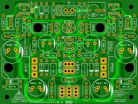
Well, I think I've arrived at a new layout I'm happy with. This is 'Revision D' which is a significant departure from my previous versions. I've decided to use the TL431 precision shunt voltage regulator as the CCS reference, with a switch to an LED CCS being an easy option for those who prefer not to source the TL431.
I'm open to constructive comments if anyone has any to offer. The layout is a 'preview' and may contain errors, error checking will take place shortly.
Attachments

Just a sugestion: instead of the KS transistors draw a board for the more available BC550/560C. 😉
Good work, great board! 🙂
Good work, great board! 🙂
I'm open to constructive comments if anyone has any to offer.
I have to apologize but your positive side CCS is nonsense.
Check out VSSA v1.4, since it offered max. performance for the price/parts count, sch available in VSSA thread.
It looks like U1 is going to try to maintain 2.499 volts between the emitter and base of Q4. Is that going to work?
Yup, screwed up there. I did not have the TL431 model handy and mistakenly used the LT1009 as a substitute in simulation. I clearly made a mistake as they are not interchangeable (the manufactures use the same schematic symbol despite their differences). This is the point of peer review. I do appreciate the reality check.
I'm not fond of JFETS largely due to increasingly poor availability (especially in through hole), greater difficulty in getting similar devices in both P and N channels and wider variations in samples of the devices. They just seem like more trouble than they are worth, but that may also be my personal lack of experience using them as I have actively avoided them.
Should be easy enough to switch to an alternative, even if that means a JFET.
Mouser has quite a few current regulator diodes, both thru-hole and SMT, in stock.
Current Regulator Diodes | Mouser
Current Regulator Diodes | Mouser
Mouser has quite a few current regulator diodes, both thru-hole and SMT, in stock.
Current Regulator Diodes | Mouser
I think the TL431 is about the quietest of them all.
Hi Jason,
congratulations on yet another nice design.
Just my 2c.
1. Is it possible to place o/p devices on same side and towards the edge ? makes it easier to mount on a narrower heat sink or can also be mounted on a perpendicular heat sink.
2. TO-126 can be either mounted on main H/S or option to have their own cute little H/S.
cant comment on the design though/ not enough knowledge.
reg
prasi
Hi Prasi,
I went with a change in orientation to allow for lower profile cases / heat sinks, something that was a comment from the earlier versions. This layout is meant to be oriented as the image shows, not vertically like the former layout. An L-bracket could likely be used for the outputs and individual heat sinks for the VAS, but my intent was direct assembly to the heat sink.
I've tried to optimize the device placement so a builder just installs it in the centre of the heat sink. I don't think there is any real reason to place the outputs on the same edge and in fact, having them spaced apart should actually improve thermal performance some. I think I get what you are suggesting but that isn't my vision here. As for the VAS devices, you could use small heat sinks and mount the devices on the component side. The question is why? A builder would already have a nice big (relatively) heat sink already, so why not use it?
VSSA - Keeping it simple
Hi Jason,
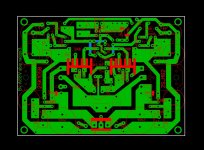
I have been following your VSSA design for a long time and think the philosophy of keeping it simple to be very important. Taking into account various improvements that have been suggested, I have re-designed your VSSA to be a single layer board with simple on-board cap multiplier. This cap multiplier does seem to work on other amps I have built and I am hoping all will be well with the VSSA too. Single layer boards are a lot easier to make at home compared to double-sided boards.
In addition the mosfets are located opposite each other and are centered on the board for physical balance and good heat sinking. The board uses an MJE340 for bias which can optionally be clipped to one of the VAS transistors for thermal temp correction.
Do you see any issues with this design?
Hi Jason,
I have been following your VSSA design for a long time and think the philosophy of keeping it simple to be very important. Taking into account various improvements that have been suggested, I have re-designed your VSSA to be a single layer board with simple on-board cap multiplier. This cap multiplier does seem to work on other amps I have built and I am hoping all will be well with the VSSA too. Single layer boards are a lot easier to make at home compared to double-sided boards.
In addition the mosfets are located opposite each other and are centered on the board for physical balance and good heat sinking. The board uses an MJE340 for bias which can optionally be clipped to one of the VAS transistors for thermal temp correction.
Do you see any issues with this design?
Attachments
Hi Jason,
I have been following your VSSA design for a long time and think the philosophy of keeping it simple to be very important. Taking into account various improvements that have been suggested, I have re-designed your VSSA to be a single layer board with simple on-board cap multiplier. This cap multiplier does seem to work on other amps I have built and I am hoping all will be well with the VSSA too. Single layer boards are a lot easier to make at home compared to double-sided boards.
In addition the mosfets are located opposite each other and are centered on the board for physical balance and good heat sinking. The board uses an MJE340 for bias which can optionally be clipped to one of the VAS transistors for thermal temp correction.
Do you see any issues with this design?
Yes, the VSSA should be kept simple. That is one reason why I have not pursued integrating front-end capacitance multipliers, or any other 'enhancements' here. Instead, I run the whole amplifier of a capacitance multiplier supply (separate project). My only concern now are the CCSs. I don't like the idea of going to the self biased JFET and I would like to remain 'symmetrical' and avoid same-sex arrangement for the positive side and negative side. This means I will likely be using either 1Q+LED or 2Q arrangements as before.
Since discovering layout software and inexpensive board houses I choose to no longer limit myself to a single sided board. Often a designer if forced into multiple compromises the two layers of copper would avoid. Not to mention advantages such as how nice a professionally made board looks, the ease of building and the overall quality being higher. I generally order boards and distribute surplus to interested folks. I used to etch at home but prefer to simply be choosier about my projects now and get boards made when I'm ready.
There is a reason my MOSFETs aren't in the middle; on a convection cooled heat sink, the middle is not the absolute best place to put them. Positioning the source of heat slightly below the centre line will yield slightly better cooling in practice. There is also no real need for temperature compensation, I just choose to mount the VAS devices to the main heat sink. They will likely run cooler that way than with smaller individual heat sinks. I haven't figured out why folks seem obsessed with using the little heat sinks when a big slab of heat sink is already available.
I have only looked at it superficially, but it looks much like PMI's design. You could possibly have posted your schematic as well. I would not have chosen to run your grounding the way you did. I got away with that on my PeeCeeBee layout but feel that I have learned a few things since then. Going for an on-board star arrangement is likely superior. Some loops also look large. Decoupling needs small loops to be effective.
My only other comments relate to the over-all aesthetic. I try and space things symmetrically and avoid the use of weird angles / geometry. I also use a relatively coarse grid (say 0.050") and only go to a smaller grid when there is absolutely no other option, and even then just to get an element or two to work. I tend to be fussy about aesthetics with this sort of stuff. You'd likely be surprised at how many iterations I go through before I even show something as a preview.
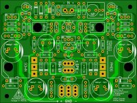
Attached is my current effort, using LED biased CCSs.
Attachments
Thanks for comments
Hi Jason,
Thanks for the constructive comments...some good things to take onboard.
I will post a schematic when I am back on my other PC, hopefully tomorrow. The design is primarily from Revision 'C' with "2Q" for the CCS. The trimmer values for the CCS are 500 R (not 285 as shown for one). I have used 47p for the VAS caps and the gate resistors for the mosfets are different to account for the device differences.
I decided to use the little heatsinks for the VAS because i have found on other amps that aligning the smaller devices under the PCB and padding them to get a good "seal" with the heatsink, since they are thinner than the mosfets, has not been satisfactory. I can always get a single "lump" of angle aluminium or copper and mount the VAS transistors to it on the top of the board instead if the two small heatsinks struggle. I don't expect them to get too hot anyway.
Your new Rev 'D' design looks good. I see that you are now using 1W 2k2 resistors for R8/9 when Rev C used 1/4 W. Did the 1/4 Watters get too hot?

Hi Jason,
Thanks for the constructive comments...some good things to take onboard.
...
I decided to use the little heatsinks for the VAS because i have found on other amps that aligning the smaller devices under the PCB and padding them to get a good "seal" with the heatsink, since they are thinner than the mosfets, has not been satisfactory. I can always get a single "lump" of angle aluminium or copper and mount the VAS transistors to it on the top of the board instead if the two small heatsinks struggle. I don't expect them to get too hot anyway.
Your new Rev 'D' design looks good. I see that you are now using 1W 2k2 resistors for R8/9 when Rev C used 1/4 W. Did the 1/4 Watters get too hot?
No need for spacers on the VAS devices. They are attached to the heat sink THEN soldered to the board. Spacing can actually be arbitrary. That's why the holes in the board are so big, so you can get to the screws without having to 'sandwich' the board and the devices.
There is no heat issue with the feedback network under normal use, but keeping the network stone cold helps with keeping things from changing in operation. Full power sine wave testing could possibly stress the feedback network with 1/4W components. It's just a little overkill, why not since it is DIY, right?
Is there any pcb for this schematic?Schematic attached as promised- "Rev C 1.?" !
Any one sided pcb is useful as we haven't paypal any more🙁
- Status
- Not open for further replies.
- Home
- Amplifiers
- Solid State
- VSSA Through-Hole Version by Jason