I have been encouraged to put the technical information for this board and layout into a separate thread. I am hoping that this will become the build thread for the Rev C circuit board, and for anyone who has my earlier Rev B version.
To give credit where it is due, the circuit design is from Lazy Cat's main VSSA thread, and inspiration for the through-hole version from Shaan and the PeeCeeBee thread. Most technical discussion and original schematics can be found there.
Schematics and BOM for the latest version will be posted here.
*** Revision C Latest Schematic and BOM ***
*** Dimensions and Mechanical Drawings ***
*** Notes on components and costs ***
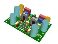
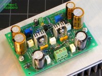
This is my third VSSA version using all through-hole parts. 4th including the SMD modules from Lazy Cat... 😀!
The main differences compared to the last revision are options for higher supply voltage and power, and options for better component and heatsink selection.
New in this revision:
Some of the test results have already been posted to the PeeCeeBee thread, the rest will be posted here soon.
I am hoping that this will become the build thread for the Rev C circuit board, and for anyone who has my earlier Rev B version.
I will do my best to keep this thread updated with test results and documentation, but new options and ideas appear in the PeeCeeBee thread almost daily, so please check there as well.
My thanks to Shaan, Lazy Cat, and various other people for their suggestions.
Special thanks to Ivan Lukic for his feedback and helping to move things along.
Links to previous threads:
http://www.diyaudio.com/forums/vendors-bazaar/225747-vssa-lateral-mosfet-amplifier.html
http://www.diyaudio.com/forums/solid-state/231662-peeceebee.html
*** Latest Update: 4.11.2013, First production boards have been ordered, 🙂 ***
To give credit where it is due, the circuit design is from Lazy Cat's main VSSA thread, and inspiration for the through-hole version from Shaan and the PeeCeeBee thread. Most technical discussion and original schematics can be found there.
Schematics and BOM for the latest version will be posted here.
*** Revision C Latest Schematic and BOM ***
*** Dimensions and Mechanical Drawings ***
*** Notes on components and costs ***
This is my third VSSA version using all through-hole parts. 4th including the SMD modules from Lazy Cat... 😀!
The main differences compared to the last revision are options for higher supply voltage and power, and options for better component and heatsink selection.
New in this revision:
- Up to 100W/channel w. +/-45V supply and specified components, and 125W/channel w. some substitutions and higher supply rails
- More space for larger electrolytic decoupling and filter caps
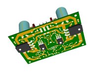
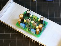
- VAS transistors top-side or bottom mounted (see 3D models below for comparison)
- More space for bigger top-side heatsinks, or a common VAS heatsink.
- Optional Jfet CCS (recommended above about +/-37V supply voltage)
- TO-3P (Renesas Latfet) or TO-247 (Semelab Alfet) devices supported
- Pads for protection diodes for ALF08P/N16-20
Some of the test results have already been posted to the PeeCeeBee thread, the rest will be posted here soon.
I am hoping that this will become the build thread for the Rev C circuit board, and for anyone who has my earlier Rev B version.
I will do my best to keep this thread updated with test results and documentation, but new options and ideas appear in the PeeCeeBee thread almost daily, so please check there as well.
My thanks to Shaan, Lazy Cat, and various other people for their suggestions.
Special thanks to Ivan Lukic for his feedback and helping to move things along.
Links to previous threads:
http://www.diyaudio.com/forums/vendors-bazaar/225747-vssa-lateral-mosfet-amplifier.html
http://www.diyaudio.com/forums/solid-state/231662-peeceebee.html
*** Latest Update: 4.11.2013, First production boards have been ordered, 🙂 ***
Attachments


Last edited:
Hey Pete,
Thanks; for starting this thread. It should help folks find things since the Peeceebee thread has become so long and has so many different layouts. You know you are dangling a big piece of meat in front of a starving dog don't you? 😀
Looking forward to building this one.
Blessings, Terry
Thanks; for starting this thread. It should help folks find things since the Peeceebee thread has become so long and has so many different layouts. You know you are dangling a big piece of meat in front of a starving dog don't you? 😀
Looking forward to building this one.
Blessings, Terry
PMI, how does this differ from LC's design apart from the obvious (TH in preference to SMT).
Also wondering how you get 100wpc from only one pair of outputs. How does the power scale into 4R loads?
Also wondering how you get 100wpc from only one pair of outputs. How does the power scale into 4R loads?
That was just a tidbit. Listening to it for days now has only increased the hunger. 😀
I'll be curious to compare these with my own as well. Nice to have a proven layout that has all the options, so it can be compliant with the PeeCeeBee or a true through hole VSSA.
@ PMI - I suppose the inclusion of these options was the reason for the 'encouragement' to take this off the PeeCeeBee thread?
Hi Pete, so this thread is very interesting...
all in one VSSA TH & SMD 🙂
there must be something new to discovered here.
Hi Ranchu,
The through hole part is easier to assembly...
the smd is not so difficult to assembly...
All is back to your parts availability & PMI know the original VSSA board by Lazy Cat is very hard to beat.
Hi Jason, I guess you should build another one & compare it to the rugged to-3 version that you already have.
Pete maybe will buy some Alfets & I might join with him 🙂
Regards
John
Last edited:
I´ve had my peeceebee running for few months now and I have new pcb with css option on a drawing board also. I am following this thread with great interest.
Good work PMI
Good work PMI
I should take this one first...PMI, how does this differ from LC's design apart from the obvious (TH in preference to SMT).
LC intended the VSSA module to fit into small spaces from the beginning, powered speakers, small multi-channel systems, etc. (so stated in his thread). I like space between components for rework, test leads, temperature probes and fat fingers... 😀
The pic below shows the previous version and LC's module, mounted on same size heatsinks, side-by-side.
- Input filter. Perhaps not required, but it is there, and I use it. LC's VSSA board is direct coupled.
- Component values in the input, feedback, and CCS are a bit different.
- VAS transistors are on top-side by default, on their own heatsinks, bottom-side as an option.
- Output bias is set by two diodes, and if necessary can be adjusted with a parallel resistor, identical to Shaan's circuit (there is no TLVH431).
- Finally and most important - the output is two conventional devices, N-channel and P-channel. LC designed for a single device with two complementary dies packaged in one TO-264.
The latfets clip as close as 3V below the rail (tested). 100W is clearly specified in LC's documentation for VSSA, with one TO-264 package, and 45V rails. So, if you have a correctly rated heatsink, and manage to keep two devices cool, it should do just fine.Also wondering how you get 100wpc from only one pair of outputs. How does the power scale into 4R loads?
You also need a reasonably clean supply, 45V with lots of ripple on top will be a no-go.
I actually look forward to some discussion about components, power dissipation, etc. in this thread. I tried to start some in the PeeCeeBee thread and did not get far.
Attachments
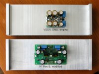
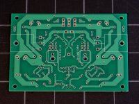
Yes, that, and the fact that even though there is just one circuit layer, the board is not strictly speaking a single-layer design, with plated holes, and solder mask top and bottom. However, it can still be built with close to the original PeeCeeBee schematic, at the lower supply voltages.@ PMI - I suppose the inclusion of these options was the reason for the 'encouragement' to take this off the PeeCeeBee thread?
Looking forward to seeing it! 🙂I´ve had my peeceebee running for few months now and I have new pcb with css option on a drawing board also...
Trying to get to it. I have almost finished testing the version with the top-side VAS transistors. I think I would like to use the ALF08N/P pair for the version with VAS on the main heatsink....
Pete maybe will buy some Alfets & I might join with him
Thank you, I am gradually working my way up to your standards... 😱Very nice looking layout PMI!
Yes the component selection is good start...I should take this one first...
....
You also need a reasonably clean supply, 45V with lots of ripple on top will be a no-go.
I actually look forward to some discussion about components, power dissipation, etc. in this thread. I tried to start some in the PeeCeeBee thread and did not get far.
1. I see some other CFA-amp use 2-3watt feedback resistor
see NX-amp by Bonsai 🙂
now where I can find these dale resistor 😀
so 0.5watt is minimum if we go for higher supply (this what I thought).
2. Input cap must be there, I've omit it & blew some 10 ohm resistor because I play to much bass 😀.
But I don't think that electrolyte the one you used is good enough, we need more option here. Big film caps also may act like an antenna...
3. 10ohm resistor dissipation (also on the zobel)
4. I'm curious what the sound with & without 10uF decoupling caps 🙂
5. Try to change VAS to another type to see how much the difference, like Jason used...
or may I change to to-220 device (driver transistor actually but easier to find) & what will happen...
Pete, sorry cos so many thoughts 🙂🙄
more to come...
Regards
The 2.2K feedback resistor was fine at 1/4 watt, up to 35V supply voltage. Probably up to 45V, because it does not see a continuous signal at high power, just during peaks. There are some better resistors one can use, low noise, higher power, same lead spacing. I am not planning on anything bigger than 1W here.Yes the component selection is good start...
1. I see some other CFA-amp use 2-3watt feedback resistor
see NX-amp by Bonsai 🙂
now where I can find these dale resistor 😀
so 0.5watt is minimum if we go for higher supply (this what I thought).
2. Input cap must be there, I've omit it & blew some 10 ohm resistor because I play to much bass 😀.
But I don't think that electrolyte the one you used is good enough, we need more option here. Big film caps also may act like an antenna...
3. 10ohm resistor dissipation (also on the zobel)
4. I'm curious what the sound with & without 10uF decoupling caps 🙂
5. Try to change VAS to another type to see how much the difference, like Jason used...
or may I change to to-220 device (driver transistor actually but easier to find) & what will happen...
Pete, sorry cos so many thoughts 🙂🙄
more to come...
Regards
There are extra pads for bigger input caps, up to 15-mm. The Nichicon bi-polar electrolytic works well, and for testing, good enough.
The Zobel is split, so you can use two resistors. Pad spacing is also wider.
Hi Pete,
Is there a schematic that matches your layout that you could post or link to? As you know I am very much in the learning stage and I would like to try to understand how the ccs works in the circuit.
Thanks, Terry
Is there a schematic that matches your layout that you could post or link to? As you know I am very much in the learning stage and I would like to try to understand how the ccs works in the circuit.
Thanks, Terry
The schematic needs some cleanup, and some component values have to be updated. It will be posted here when I am done testing. The CCS works the same as the one shown in V1.4 of Lazy Cat's schematic. It takes the place of the resistor which has been variously posted as 15K, 18K, etc. in the other thread. It keeps the current close to constant ~2 mA over a wide range of supply voltage. You can just google "Jfet CCS" there are plenty of detailed examples and explanations, much better than anything I can post.Hi Pete,
Is there a schematic that matches your layout that you could post or link to? As you know I am very much in the learning stage and I would like to try to understand how the ccs works in the circuit.
Thanks, Terry
Since I know you have a Variac to test with, you can try changing your supply voltage up and down 10% or so, and measure the VAS current. You will probably observe that it varies with the supply voltage more than one might expect. With the CCS, mine stays pretty close to the 12-13 mA, where I set it.
Sent ya PMs PMI. SOrry for the delay on the cap multis stuff. Want 6 of these as well if ya got 'em!!
The latfets clip as close as 3V below the rail (tested). 100W is clearly specified in LC's documentation for VSSA, with one TO-264 package, and 45V rails. So, if you have a correctly rated heatsink, and manage to keep two devices cool, it should do just fine.
You also need a reasonably clean supply, 45V with lots of ripple on top will be a no-go.
I actually look forward to some discussion about components, power dissipation, etc. in this thread. I tried to start some in the PeeCeeBee thread and did not get far.
Thanks for that explanation. Looking at the SOA graph for the ALF08N, it seems that ~100W is around the limit for a single pair. Do you need some sort of current limiting to drive 4R loads to peak power with 45VDC rails?
Has there been any discussion about doubling the OPS to 2 pairs?
Last edited:
Can't use a single pair at 45V into 4 ohms. Not as it stands. You have to lower the voltage. You might be able to use the double-die TO-264 ALF16. The dies are matched at the factory when they put them in the package. Have not tried that yet, it will most likely need some other component value changes. It will be more difficult to mount on the heatsink, because the mounting hole will be just outside the board outline.Thanks for that explanation. Looking at the SOA graph for the ALF08N, it seems that ~100W is around the limit for a single pair. Do you need some sort of current limiting to drive 4R loads to peak power with 45VDC rails?
Has there been any discussion about doubling the OPS to 2 pairs?
Yes, two pair has been talked about, in the PeeCeeBee thread, and a layout has ben posted by Shaan. John Bali is working on one.
What would you recommend as a suitable max into 4R? About 35VDC?
Would be interested in some boards if you end up doing a run. Interesting to compare with LC's VSSA amp, which I have almost completed and will post details in his thread soon.
Would be interested in some boards if you end up doing a run. Interesting to compare with LC's VSSA amp, which I have almost completed and will post details in his thread soon.
30~35V into 4 ohms, if you want to stay safe, but you could push it quite a bit, if you wanted to. With care, you can make some assumptions about the average current, and calculate back from that. most people want the extra power for dynamic range, not to blast out a continuous 1KHz sine wave at maximum power (chuckle).What would you recommend as a suitable max into 4R? About 35VDC?
Would be interested in some boards if you end up doing a run. Interesting to compare with LC's VSSA amp, which I have almost completed and will post details in his thread soon.
edit:
I am planning on making a couple small board orders, and for now I am just keeping a list of interested people.
Last edited:
- Home
- Amplifiers
- Solid State
- VSSA Through-Hole-PCB build thread