The design idea originally featured in my diyaudio blog.
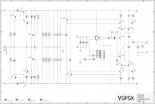
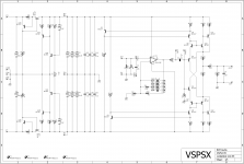
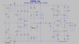
It's the single op amp IC phono stage of the VSPS, with a discrete solid state buffer and shunt-source voltage regulator.
In this thread, we'll develop the board layout, get some boards made, and offer a special "guinea pig" trial of boards/parts to anyone interested in building their own over the holidays.
So first off time to fire up Eagle 7.7.0 and get busy with the layout.
Latest LTSpice version attached. Part numbers not consistent with BOM.
Attachments
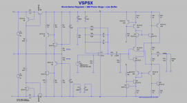
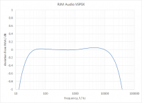
By the way I decided to removed the Allen Wright 50 kHz time constant from the VSPS circuit for this iteration. The response still tips up in the ultrasonic since the op amp is non-inverting, but at much higher frequencies than before.
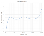
Simulated RIAA response measured at the buffer output is +/- 0.2 dB 20Hz-60kHz.
Simulated RIAA response measured at the buffer output is +/- 0.2 dB 20Hz-60kHz.
Attachments
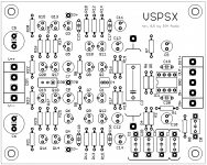
rev. 0.4
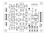
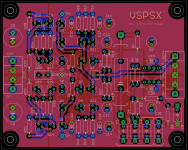
Complete board, ERC DRC passed.
* tweaked the RIAA values and added a LP filter to the output to give a more conventional treble response with balanced bass/treble rolloff.
* added optional input resistor and capacitor to for cartridge matching.
* the trim pot. adjusts the balance of V+ and V-, so they can be made equal. The absolute output voltage |V+| + |V-| will be about 24 V and is fixed.
* board is "new RJM 80x100 protocol" which shares M3 70x90 mm mounting holes with the Sapphire and CrystalFET boards, but not the older VSPS300 and Phonoclone boards.
* board can be easily converted to line stage or mic preamp use
* before you ask, no: 2520 modules and discrete opamps will not be supported. Both because of size constraints, and because the power supply is set for the ~5 mA of a typical IC, not the 25-50 mA of most modules.
Attachments
What circuits is necesarry to replace/remove to make this preamp line level, without phono correction?
Remove C1, C2, and R4. Change R5 to about 4k75. Change R2 to 2k2 or as needed for the desired gain as A = R5/R2+1. That's it.
Of course you'd have to interface it to the volume control, input selector, etc. The circuit is only the gain stage and output buffer.
Of course you'd have to interface it to the volume control, input selector, etc. The circuit is only the gain stage and output buffer.
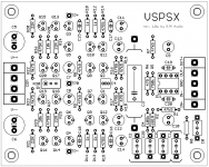
Since I'm here, I might as well post rev. 05.
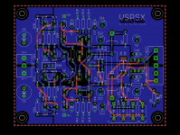
* some cleaning up of the layout traces, moving as much as possible to the bottom layer.
* added second COM. The extra pad simplifies connecting dual bridge rectifiers.
* minor cosmetic changes
Seems like it's done, so I'll bump it up to rev. 1.0 and send to fabrication after a final once-though.
* some cleaning up of the layout traces, moving as much as possible to the bottom layer.
* added second COM. The extra pad simplifies connecting dual bridge rectifiers.
* minor cosmetic changes
Seems like it's done, so I'll bump it up to rev. 1.0 and send to fabrication after a final once-though.
Attachments
hi,
any change in the handling of ticks and pops with such a change?
mlloyd1
any change in the handling of ticks and pops with such a change?
mlloyd1
By the way I decided to removed the Allen Wright 50 kHz time constant from the VSPS circuit for this iteration. The response still tips up in the ultrasonic since the op amp is non-inverting, but at much higher frequencies than before.
Simulated RIAA response measured at the buffer output is +/- 0.2 dB 20Hz-60kHz.
Perfect timing! I came into the forum today looking for a new phonostage to build.. Ill be following closely 🙂
hi,
any change in the handling of ticks and pops with such a change?
This is mostly determined by headroom, which for the VSPSX is average-to-good and unchanged from the VSPS. Information above 20 kHz is more attenuated however - this may have some subjective benefit.
rev. 1.0a
* added brestrict fill and removed gnd fill on bottom layer
* added or fixed component values (R21, R28, R30)
* updated ltspice circuit to be have component names consistent with board
* trivial changes to component and layout placement, silk screen
* created BOM
* added brestrict fill and removed gnd fill on bottom layer
* added or fixed component values (R21, R28, R30)
* updated ltspice circuit to be have component names consistent with board
* trivial changes to component and layout placement, silk screen
* created BOM
Attachments

A question: does it really sound better with the buffer than without?
Always assumed the primary purpose of a buffer following an opamp in a phono stage is to drive a low impedance riaa network. A 1m cable should be within the abilities of any old opamp. Unless it does sound better to you this way.
Always assumed the primary purpose of a buffer following an opamp in a phono stage is to drive a low impedance riaa network. A 1m cable should be within the abilities of any old opamp. Unless it does sound better to you this way.
It was a related case, using the phonoclone with and without the bboard rev. 1.1a, but yes, I did feel it sounded warmer and fuller with the buffer.
The usual hand-waving argument is that while an op amp is of course capable of driving 1m interconnects, the buffer isolates the opamp from the capacitance and inductance of the cable network, reducing the likelyhood of instability in the form of overshoot and ringing and what not. I have no supporting evidence, but I'm willing to buy it, personally. Op amp ICs tend to sound better the less work they have to do. Probably the limp output bias current is something to do with it.
But - since we're on the subject - integrating the buffer into the VSPS circuit like this provides two incidental benefits. The first is the grunt output of the buffer means we can add a LP filter to the output and still keep the output impedance low. The second is the coupling capacitor can be moved from the output to the interstage, and since the buffer section has a fixed, known impedance the capacitor can now be made 4-5 times smaller than the 2.2uF it was previously. The low impedance, DC coupled output of the buffer will power low impedance loads (down 600 ohms) with no additional bass rolloff and/or need for giant coupling caps.
That last point is kinda a biggie.
Last edited:
So... rev. 10a has been sent for fabrication. 10 pcs, so 5 sets. I get one, 4 left to send out to lucky Guinea pigs. Prototype boards, basic green with white stencil - no go-fast racing stripes.
Cost of the boards (set of two) will be nominal $10 to cover shipping and paypal.
I can provide some or all the parts, but not below cost. Mouser pegs the single quantity BOM at ~$80 and you are welcome of course to order from there.
PM me if interested, first come first serve as they say. Boards should ship in 2 weeks.
Sorry my turntable is dead so I cannot participate right now. I will follow the thread with interest though.
So I suppose I should set out the stall and make a pitch as to why this is the greatest phono stage ever etc. etc.
The truth is it is unlikely I will ever get a chance to listen to it. I use a moving coil cartridge and am very happy with the CrystalFET.
As a reliable and convenient general-purpose MM phono stage however the VSPSX has a lot going for it. Let me explain -
I've already touched on the buffer advantages, but to recap: low distortion, high PSRR, plenty of class A output bias, drives the LP filter, isolates the op amp and coupling cap from the output load. Smaller coupling capacitor needed as a result. The buffer circuit is derived from the Sapphire3, and is anyway a known quantity, brute force no tricks kind of topology.
The VSPS circuit itself is a known quantity, hundreds have been built. An op amp IC voltage stage is not the most exotic idea, true, but as a means to an end it you could do a lot worse. It does the job. The RIAA eq. is very accurate, LTSpice allows fine tuning the total response and the VSPSX makes full advantage of that. Use 1% resistors, 1% mica caps, it's about as good as it gets for midband RIAA accuracy.
So that leaves the voltage regulators, which is the most experimental part of the circuit. I used them in the CrystalFET already, although that was with MOSFETs I thought the result sounded excellent and was anxious to pursue the concept further. The best way to describe shunt regulators is like having a counterweight on an elevator exactly balancing the weight of the carriage. There is almost no work left to do by the driving motor compared to lifting the carriage alone, and, as such, no imprint of the signal current gets transmitted back towards the power supply past the shunt element. This means quieter voltage rails with less likelihood of crosstalk or intermodulation. I've actually seen this in action in LTSpice - it's quite fascinating, and totally sold me on shunts. The voltage regulator is a simple 4 transistor design and provides about 80 dB of ripple rejection across the audio spectrum. Soft-start and overcurrent protection are intrinsic to the design. The trim pot. allows the positive and negative output rails (V+, V-) to be adjusted to exactly the same magnitude, for those of you that care about these things.
(If you are wondering the reason this voltage regulator will never replace an LM7812 is that the config is only good up to about 50 mA, and the whole thing must be set up for a given load current and output voltage. Pull more than the set output current and the regulator stops working. Not good! It's therefore only really practical when it's incorporated into a circuit where the load current limit can be guaranteed.)
Last edited:
The truth is it is unlikely I will ever get a chance to listen to it. I use a moving coil cartridge and am very happy with the...
You need to go AD797 😀
Resistance is futile...
Last edited:
- Home
- Source & Line
- Analogue Source
- VSPSX very simple phono stage + x