From a physical standpoint the board should handle it, with a nice ground plane and ceramic and electrolytic caps right next to the DIP socket.
That reminds me (your intention, I suppose?) of a certain someone who used an AD797 in the VSPS set up for MC gain. That idea might be worth revisiting again in the context of the VSPSX...
That reminds me (your intention, I suppose?) of a certain someone who used an AD797 in the VSPS set up for MC gain. That idea might be worth revisiting again in the context of the VSPSX...
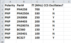
I'd like to ask, why were the BC327/337 transistor types chosen? Rather than, say, BC550/560 or 2SC1845/2SA992? And also, why choose the -25 beta grade rather than the -40 beta grade?
Thank you.
Thank you.
Yep I was one of those using ad797 🙂
It makes the buffer a bit redundant though. Apart from the extra low pass filter.
It makes the buffer a bit redundant though. Apart from the extra low pass filter.
@Mark
BC337/327 are cheap and widely available, and I was told they sound better than the BC550/560. The mid-range hfe grade (25) was chosen as a balance of transconductance and device spread.
The discrete transistors used in the circuit are in applications which are not particularly sensitive to the device parameters. The critical transistors are the ones in the op amp IC.
Textbooks say that transconductance of a BJT depends upon collector current and nothing else:The mid-range hfe grade (25) was chosen as a balance of transconductance and device spread.
- gm = Ic / ( kT/q)
Are the textbooks wrong? Does the BC337-25 have a different transconductance than the BC337-40 when both devices operate at the same current?
I was thinking of current gain and wrote transconductance. Sorry.
To be honest, as long as the Vbe are clustered reasonably close I don't think it matters which you use. Every transistor in the circuit is configured as a follower.
To be honest, as long as the Vbe are clustered reasonably close I don't think it matters which you use. Every transistor in the circuit is configured as a follower.
Thanks for your reply! I think I might describe the circuit by saying it contains not one but three configurations of transistors: (a) followers; (b) 2T shunt feedback current sources (2 x CommonEmitter); (c) Complementary Feedback Pairs (CC+CE = Sziklai).
In my experience the 2T shunt feedback current source configuration (like Q13+Q15 in post #10) has a tendency to oscillate when base stopper resistors are not included {as you did not}. In my experience some transistor types have a greater propensity to oscillate in this circuit, and other types have a lesser propensity to oscillate in the 2T shunt feedback current source. I wonder, perhaps the person who told you the BC337 "sounds better" (post 24) than the BC550 was describing the difference between an oscillating current source, and a not-oscillating one.
Since the buffer is not enclosed in the opamp's DC feedback loop, the buffer's offset voltage is not attenuated by NFB. It is directly presented at the output. So you want good matching between the upper half of the buffer circuit and the lower half. In particular you want the two current sources to be identical, which means (PNP_VBE_Q3 / R10) should be exactly equal to (NPN_VBE_Q4 / R11). Perhaps the BC327/337 types have better matching between NPN_VBE and PNP_VBE, than the BC550/560.
Still, it's a happy situation for builders to only purchase one device-type for all NPNs and one device-type for all PNPs. It's also a happy situation that the BC327 has an absolute maximum rating of 800 milliamps (!) compared to only 100mA for the BC550. Even though your Q15-R20 current source runs the whole circuit at ~ 30-35 mA at the most, it's pleasantly comforting to have an enormous margin of safety.
Thanks for your comments.
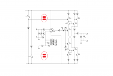
Just to double check, you are advising adding four resistors marked on the scheme below?
I've seen schematics both with and without, usually without. The Sapphire3 uses the same layout and I've not had any obvious problems with stability. Any thoughts on what's the best way to check?
Just to double check, you are advising adding four resistors marked on the scheme below?
I've seen schematics both with and without, usually without. The Sapphire3 uses the same layout and I've not had any obvious problems with stability. Any thoughts on what's the best way to check?
Attachments
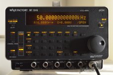
I'd use an oscilloscope to view the voltage at the emitter of the current source transistor (Q5-Q6), and again at the base of the current source transistor. Apply a 50 kHz square wave to the amplifier input* and adjust its amplitude to get maximum output just before clipping. Search for ringing around the leading edge and falling edge. If you see ringing, yikes, take corrective action.
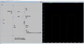
I think it would be cheap insurance to lay out the PCB including eight base stopper resistors. If that adds too much area, you can orient them vertically which reduces the footprint to 0.1" by 0.2". The stoppers are in series with the bases of Q13-Q16, and Q3-Q6 (designators in post 10 schematic, 4th image). Then if testing shows that you need base stoppers, you don't have to re-spin the PCB. If you don't need them, connect jumpers.
*I guess this would be sqwave -> inverse RIAA -> input. Or else perform the square wave tests before populating the capacitors in the opamp feedback network.
That sounds do-able. I can use the Sapphire as that has a linear input stage.
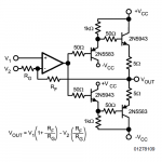
By the way when I first built the buffer I followed an obscure TI app note with all the base resistors included as shown below. It sounded fine, but the next one I built without the resistors, as per LH0002 etc. It also sounded fine. So I guess I stopped worrying about it.
By the way when I first built the buffer I followed an obscure TI app note with all the base resistors included as shown below. It sounded fine, but the next one I built without the resistors, as per LH0002 etc. It also sounded fine. So I guess I stopped worrying about it.
Attachments
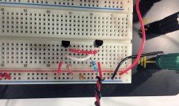
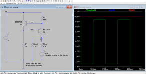
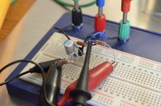
This little 2T CCS oscillated on my carefully laid out PCB so I copied it over to the solderless breadboard for further experiments. Here are a couple images. It oscillates on the solderless breadboard too.
Q2 is on the left in the photo, Q1 is on the right
node EEE is the white horizontal wire
node BBB is the red horizontal wire
left resistor (brown body) is 12K
right resistor (blue body) is 154R
yellow blob is 0.1uF ceramic cap (supply bypass)
_
Q2 is on the left in the photo, Q1 is on the right
node EEE is the white horizontal wire
node BBB is the red horizontal wire
left resistor (brown body) is 12K
right resistor (blue body) is 154R
yellow blob is 0.1uF ceramic cap (supply bypass)
_
Attachments
I have that exact same breadboard &c so let me see if I can reproduce that.
Meanwhile, since you have that set up - what value resistors do you need where to kill that ringing? Does it make any difference if the transistors are placed closer together, or the bypass capacitance is increased?
Thanks,
Meanwhile, since you have that set up - what value resistors do you need where to kill that ringing? Does it make any difference if the transistors are placed closer together, or the bypass capacitance is increased?
Thanks,
I decided that the parts count for the "repaired" 2T shunt feedback current source, was higher than the parts count for other current source designs. So I don't use the 2T shunt feedback current source with base stoppers myself, and I don't have recommended resistor values to suggest. Very sorry. A very crude "severe overkill" rule of thumb might be: make the RC timeconstant of (BaseStopper x TransistorCbc) greater than 6 nanoseconds. This corresponds to a pole at 25 MHz, far less than the oscillation frequency on the scope trace. And also, far less than the fT of the small signal transistors you're likely to use. But remember: I haven't tried this rule-of-thumb myself, in the lab. It's just an opinion.
Instead I tend to gravitate towards variations upon the theme of 3 diodes + 2 resistors + 2 transistors in cascode. For example posts #72 and #34 in this thread
Instead I tend to gravitate towards variations upon the theme of 3 diodes + 2 resistors + 2 transistors in cascode. For example posts #72 and #34 in this thread
Last edited:
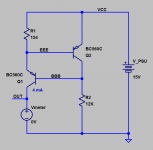
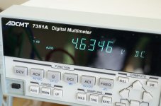
Just noticed this in the figure in #32: Only two resistors shown, so what is the value of the load resistor used to sink the 4 mA?
Last edited:
Just the resistance of the ammeter shunt which, at 4mA, is probably in the neighborhood of 50 ohms. The collector is tied to ammeter+ and ground is tied to ammeter-. The schematic shows this as "Vmeter". The red and black twisted pair in the photo, go to the ammeter.
Last edited:
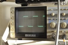
It's quiet as a sleeping baby when I try it. Exactly as simulated.
I'm just measuring DC operation though, at the output, I haven't forced an excitation like the square pulse shown in the sim, nor did I check TP1/TP1 (EEE/BBB). What did you do to get it to oscillate?
I'm just measuring DC operation though, at the output, I haven't forced an excitation like the square pulse shown in the sim, nor did I check TP1/TP1 (EEE/BBB). What did you do to get it to oscillate?
Attachments

Last edited:
Here's what I did
1. Plug in two Fairchild BC550Cs, two resistors, and one ammeter
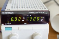
2. Apply 15VDC
3. Probe every collector, every base, and every emitter
1. Plug in two Fairchild BC550Cs, two resistors, and one ammeter
2. Apply 15VDC
3. Probe every collector, every base, and every emitter
No, nuffink.
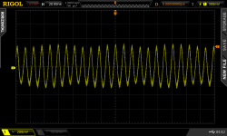
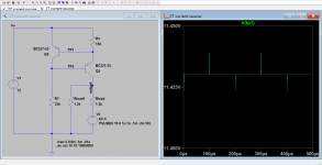
It's all clean, no trace of anything whatsoever at static bias. Finally I drove the output with a 16V p-p 50 kHz square wave, as shown in the schematic. The output goes from about 2 to 10 V. Clean as a whistle, exactly as simulated. TP1 and TP2 show minute spikes on the rising and falling edges with no ringing whatsoever, again as shown in the simulation.
/end investigation
Attachments
- Home
- Source & Line
- Analogue Source
- VSPSX very simple phono stage + x