Made some nice progress this week, actually tested / biased both halves of the amplifier channel.
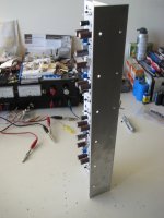
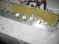
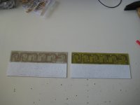
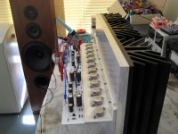
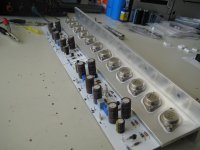
I spray painted the PCB's white. Gives a nice look better then the two discolored PCB's.
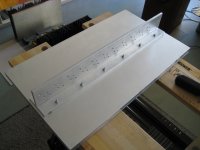
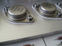
Mounted all components. Mounted all FET's with mica and goop...lots of work🙂
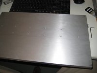
With first testing it seems like the heat is getting easy of the VFETs and off the T-bar to the 15mm ALU sheet. So that looks promising.
That heat was my biggest problem with the VFET CSX1.
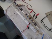
Initially some problems with a big startup current which results in a limiting lab PSU. I had them at 1 ampere for testing purpose. After setting the lab supply to 4 amps the output stage started.
I changed the C1 and C2 to 470uF and R37/R38 to 2k21 ( Teabag/Botte mod), much better, lower startup current through the VFET's.
I did see Papa has changed C3 and C4 to 47uF instead of 220uF in the last DIY VFET schematic. So I must try that also.
Also the voltage at the VFETs is about 18.7 Volts.... a bit low, so I must play with R13 and R14 to get them a bit higher.
For testing I put in some 0.1 Ohm source resistors to see if the current is evenly distributed, and it was. The VFET's were matched some time ago, so that was expected...
I have a lot of pictures😀🙂
I spray painted the PCB's white. Gives a nice look better then the two discolored PCB's.
Mounted all components. Mounted all FET's with mica and goop...lots of work🙂
With first testing it seems like the heat is getting easy of the VFETs and off the T-bar to the 15mm ALU sheet. So that looks promising.
That heat was my biggest problem with the VFET CSX1.
Initially some problems with a big startup current which results in a limiting lab PSU. I had them at 1 ampere for testing purpose. After setting the lab supply to 4 amps the output stage started.
I changed the C1 and C2 to 470uF and R37/R38 to 2k21 ( Teabag/Botte mod), much better, lower startup current through the VFET's.
I did see Papa has changed C3 and C4 to 47uF instead of 220uF in the last DIY VFET schematic. So I must try that also.
Also the voltage at the VFETs is about 18.7 Volts.... a bit low, so I must play with R13 and R14 to get them a bit higher.
For testing I put in some 0.1 Ohm source resistors to see if the current is evenly distributed, and it was. The VFET's were matched some time ago, so that was expected...
I have a lot of pictures😀🙂
Attachments
-
 IMG_6025ww.jpg272 KB · Views: 1,409
 -
 IMG_6047ww.jpg254.8 KB · Views: 839
 -
 IMG_6046ww.jpg289.6 KB · Views: 860
 -
 IMG_6042ww.jpg395 KB · Views: 606
 -
 IMG_6041ww.jpg297.4 KB · Views: 656
 -
 IMG_6039ww.jpg381.2 KB · Views: 609
 -
 IMG_6035ww.jpg322.7 KB · Views: 1,206
 -
 IMG_6034ww.jpg197.7 KB · Views: 1,256
 -
 IMG_6033ww.jpg246.5 KB · Views: 1,299
 -
 IMG_6026ww.jpg244.4 KB · Views: 1,369
Kraftman work & beauty.
I guess Walter you are excited to get step by step first music notes
front balanced mini Vfet monster haha 😀
Most excellent DIY i like it and dream about 🙂
Fascinating thread btw.
Kindest regards
I guess Walter you are excited to get step by step first music notes
front balanced mini Vfet monster haha 😀
Most excellent DIY i like it and dream about 🙂
Fascinating thread btw.
Kindest regards
A new Milestone
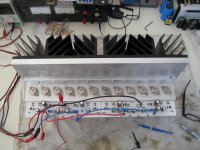
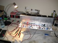
This is what I wanted to check: can the heatsinks, alu sheet combination dissipate all the heat when running each VFET at 1 Ampere?
And yes it can 😀🙂 I'm happy.
I can continue building at a slower pace...
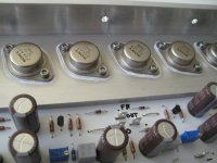
This heatsink is monstrous, it's a whole other league, it's Pass labs vs. Firstwatt.... Wow.
I mounted the T-bar on the Alu sheet and the heatsinks on the Alu sheet for initial testing, without further polishing or cooling paste, so things can only get better.
Better conducting of the heat and thus cooler transistors.
As you can see in the picture it's dissipating 28x2x4= 224 Watts.
After one hour heatsinks are around 48 degrees, T-bar around 54 and the top of the VFETs around 62 degrees.
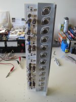
And yes on the last picture it is slowly starting to look as the real '40 years Anniversary Sony VFET amp'
This is what I wanted to check: can the heatsinks, alu sheet combination dissipate all the heat when running each VFET at 1 Ampere?
And yes it can 😀🙂 I'm happy.
I can continue building at a slower pace...
This heatsink is monstrous, it's a whole other league, it's Pass labs vs. Firstwatt.... Wow.
I mounted the T-bar on the Alu sheet and the heatsinks on the Alu sheet for initial testing, without further polishing or cooling paste, so things can only get better.
Better conducting of the heat and thus cooler transistors.
As you can see in the picture it's dissipating 28x2x4= 224 Watts.
After one hour heatsinks are around 48 degrees, T-bar around 54 and the top of the VFETs around 62 degrees.
And yes on the last picture it is slowly starting to look as the real '40 years Anniversary Sony VFET amp'
Attachments

Last edited:

Woweh!
Walter, what a great project this is.
This amp won't blow around in the wind.
I am following you as this is something I also might end up building, when time allows.
Great inspiration from you (and of course also from the chi master himself, the one and only NP). Thank you.
Walter, what a great project this is.
This amp won't blow around in the wind.
I am following you as this is something I also might end up building, when time allows.
Great inspiration from you (and of course also from the chi master himself, the one and only NP). Thank you.
Yeah, thanks... I wonder if this amp will ever leave my room, I certainly won't move it downstairs on my own, needs some friends help 🙂
What I like about these VFET output stage is that when they heat up the bias gets a bit lower. Not like the F5T which gets higher and higher when warming up.
So no thermal runaway...
What I also like is that the output offset stays so low, about 15 mV difference between cold start and completely heated up. I have never experienced such stable behavior with my amps.
I'm still fiddling with my startup behavior, lowering C5 and C6 from 220uF to 100uF makes a big difference, much lower initial current flow through the VFETs.
It's a pity I'm out of 47uF Elna Silmic caps. Have to order and try those.
Yeah, thanks... I wonder if this amp will ever leave my room, I certainly won't move it downstairs on my own, needs some friends help 🙂
hahaha, I'm in the same situation with my multiple Aleph J in one chassis. I think I'll build mono block next time just for this reason...🙂
Smaller monoblocks will be easier on your back, but they probably won't look as cool 🙂
Can't wait to see when you're finished. This will be one impressive amp.
Can't wait to see when you're finished. This will be one impressive amp.
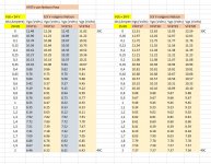
I have been matching and selecting pairs for my VFET amp and need some experts vision...
The VFET pairs are measured like this:
Ids (Ampere) Vgs (Volts)
2SK82 VFET#10 VFET#9
0 11.28 11.03
0,05 10.69 10.53
0,1 10.40 10.32
0,15 10.17 10.15
0,2 9.98 9.98
0,25 9.82 9.84
0,3 9.67 9.71
0,35 9.54 9.58
0,4 9.41 9.46
0,45 9.30 9.34
0,5 9.18 9.22
0,6 8.97 8.99
0,7 8.75 8.78
0,8 8.55 8.56
0,9 8.35 8.34
1 8.15 8.12
1,1 7.96 7.91
1,2 7.77 7.70
1,3 7.58 7.49
1,4 7.38 7.28
1,5 7.20 7.07
1,6 7.00 6.85
1,7 6.81 6.65
1,8 6.62 6.43
1,9 6.42 6.22
2 6.24 6.02
I am selecting which VFET-pairs goes in which side of the channel, and also which N-channel matches best with which P-channel pair.
They will be biased around 1 Ampere.
So I can look at a pair and see how much voltage is needed to go from 0.5 to 1.0 Ampere and how much from 1.0 to 1.5A.
Or if I look from 0.5 to 2.0A, I can come up with a value of how much different the Vgs must be, to move from 0.5 to 2.0A.
Above it is around 3.1 Volts to give a 1.5 Ampere change.
This value tells me something about the curves of the devices.
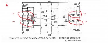
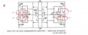
I have done this with all my pairs, and now the big question is: What is better?
Picture A or picture B?
Picture A both sides, left and right, are the same but between N and P there is a difference.
Or like picture B, left side is perfect, only the right side is imbalanced?
With better I mean: in the context of distortion and harmonic cancellation.
This is for one channel only. The other channel has all 3.2V in all quadrants🙂
Thanks to the perfectly matched VFETs from Mr. Pass 😀
I will post some curves soon, unbelievable....
I hope someone can answer....
The VFET pairs are measured like this:
Ids (Ampere) Vgs (Volts)
2SK82 VFET#10 VFET#9
0 11.28 11.03
0,05 10.69 10.53
0,1 10.40 10.32
0,15 10.17 10.15
0,2 9.98 9.98
0,25 9.82 9.84
0,3 9.67 9.71
0,35 9.54 9.58
0,4 9.41 9.46
0,45 9.30 9.34
0,5 9.18 9.22
0,6 8.97 8.99
0,7 8.75 8.78
0,8 8.55 8.56
0,9 8.35 8.34
1 8.15 8.12
1,1 7.96 7.91
1,2 7.77 7.70
1,3 7.58 7.49
1,4 7.38 7.28
1,5 7.20 7.07
1,6 7.00 6.85
1,7 6.81 6.65
1,8 6.62 6.43
1,9 6.42 6.22
2 6.24 6.02
I am selecting which VFET-pairs goes in which side of the channel, and also which N-channel matches best with which P-channel pair.
They will be biased around 1 Ampere.
So I can look at a pair and see how much voltage is needed to go from 0.5 to 1.0 Ampere and how much from 1.0 to 1.5A.
Or if I look from 0.5 to 2.0A, I can come up with a value of how much different the Vgs must be, to move from 0.5 to 2.0A.
Above it is around 3.1 Volts to give a 1.5 Ampere change.
This value tells me something about the curves of the devices.
I have done this with all my pairs, and now the big question is: What is better?
Picture A or picture B?
Picture A both sides, left and right, are the same but between N and P there is a difference.
Or like picture B, left side is perfect, only the right side is imbalanced?
With better I mean: in the context of distortion and harmonic cancellation.
This is for one channel only. The other channel has all 3.2V in all quadrants🙂
Thanks to the perfectly matched VFETs from Mr. Pass 😀
I will post some curves soon, unbelievable....
I hope someone can answer....
Attachments
Last edited:
Walter,
Thanks so much for your posts!
I'm trying to do something like what you're doing, by making my own single-sided PCBs
I'm greatly enjoying your project progress and photos.
I wanted to alert you to something discovered while tracing circuit paths and comparing Papa's schematics and PCB art with your PCB layout.
You may well have already caught it after the pictures were taken, but the trace for the shorted leads of the P1 bias-pot should go to Ground, not the trace for the single lead.
Would you please share some info and pictures regarding the Front End PCB also?
Is that PCB available for purchase somewhere, or did you design and make that one too?
Thanks.
Respectfully,
Msr. Mojo
Walter in the A you have no offset....
Anyway the transistors VFETs are overwhelmed paired
Sadly....
Anyway the transistors VFETs are overwhelmed paired
Sadly....
I wanted to alert you to something discovered while tracing circuit paths and comparing Papa's schematics and PCB art with your PCB layout.
You may well have already caught it after the pictures were taken, but the trace for the shorted leads of the P1 bias-pot should go to Ground, not the trace for the single lead.
Hi Mojo, I saw that, but it really makes no functional difference whether they go to ground or to the TL431. You are only setting a certain resistor value. This kind of connecting is done, so you don't get hiccups when the wiper loses contact with the carbon or plastic film.
I will post some more photo's of the frontend later on, I made the PCBs myself indeed.
Walter in the A you have no offset....
Anyway the transistors VFETs are overwhelmed paired
Sadly....
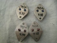
Look at the insane matches I got from the DIYAudio store:
Especially those 4 2SJ28's .... WOW exact matches, curve traced 😀
And you know how much they differ normally.
I think they are sequentially picked from the boxes and those 4 are cut from the same die.
While measuring them, I checked more than once if I was measuring the same VFET over and over again 🙂😛
I'm a lucky guy this time....
Attachments
Tell with confidence, how it sound Walter?
Does still the CSX1 is your favorite sound amp?
Bst RGRDS
Does still the CSX1 is your favorite sound amp?
Bst RGRDS
Yup, no idea how this amp will sound, still a long way to go before I can listen to it.
I've never heard a balanced build, very curious.
CSX1 is playing again, right now😉
I've never heard a balanced build, very curious.
CSX1 is playing again, right now😉
Look at the insane matches I got from the DIYAudio store:
Not surprising, they were in the original flats taken in sequence, so there was
a good chance of getting the same die, and they were all tested on a
temperature regulated 50 deg heat sink and then sorted by Vgs.
Looking at large numbers of them, there is great consistency. Of the 2000
or so I tested, I had one bad one.
The matching was all Papa's doing. We just loaded them in the kits in the sequence he had packed them..
- Home
- Amplifiers
- Pass Labs
- VFET-X (or my 1/3 40th Anniversary Sony VFET Clone)