You don't have to rely on the provided libraries, it is dead easy to create custom components in design spark.
Sent from my iPhone using Tapatalk
Cool. I'll look into making some models eg lateral mosfet, toshiba jfet etc.
First update
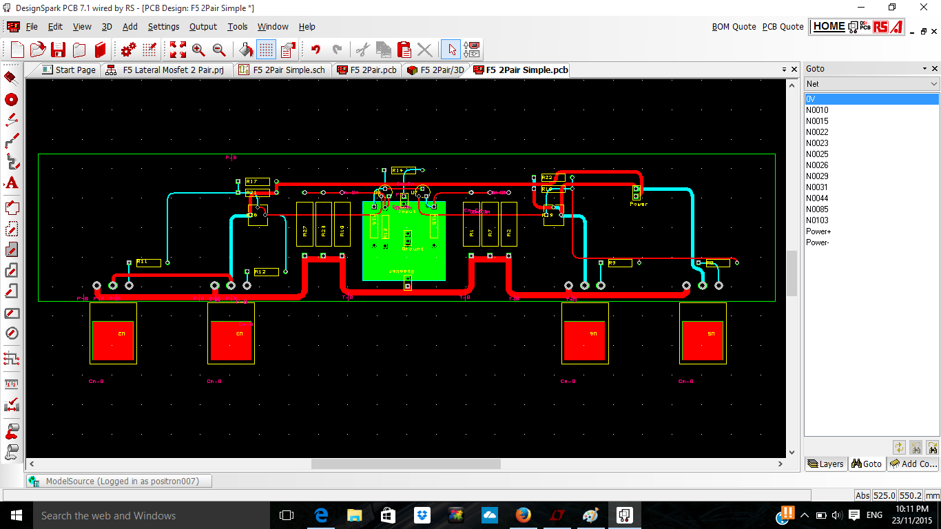
1) Zero Vias
2) Added copper pour for ground/0V
3) Adjusted pad size on mosfets
Still more to do. Not entirely happy with dc power routing.
1) Zero Vias
2) Added copper pour for ground/0V
3) Adjusted pad size on mosfets
Still more to do. Not entirely happy with dc power routing.
The name of such kind of areas is power plane! So, yes, for all signal carying power. A second nice effect is the thermal characteristics!
I´m sure that´s possible to route all signals on one PCB side with better placement (perhaps R8 180°?).
Can you PM me a PDF of your schematics?
Jean-Paul
I´m sure that´s possible to route all signals on one PCB side with better placement (perhaps R8 180°?).
Can you PM me a PDF of your schematics?
Jean-Paul
I had intended on spying on those, but haven't had a chance as yetobserve pictures of FW pcbs and learn
The only dimensionnig features are heat spreading and the UMS: good start for layouting, you´ve the dimension of the board including mounting holes and the placement for the mosfets.
Start with the schematics and choosing your favorite components (or manufaturers).
Go to layout:
- gate resistors as near as possible to the mosfet gate (FW PCB´s don´t care!),
- don´t use mounting holes for power supplying,
- output as power plane: output connector with ground is nicely placed,
- they are no fixed rules for analog PCB routing, you need a great experience.
Isn´t simple to describe PCB routing with only text and bullets!
But sorry 2 picoDumbs, there is a lot change before you can think about manufacturing!
Tête haute et bon courage!
P.S.: I´m not a fan of spying but it is a good starting point - learning by doing...
Jean-Paul
Gate resistors are 3mm away.Go to layout:
- gate resistors as near as possible to the mosfet gate (FW PCB´s don´t care!),
- don´t use mounting holes for power supplying,
- output as power plane: output connector with ground is nicely placed,
- they are no fixed rules for analog PCB routing, you need a great experience.
List 3 things that need to be changed.
To the OP: one of your mates down under has put together a nice tutorial on laying out PCBs. Check out David Jones's EEV Blog. Dave's an interesting character. 🙂
PCB Design & Layout Tutorial - Learn how to design a professional PCB!
PCB Design & Layout Tutorial - Learn how to design a professional PCB!
I'll read it.To the OP: one of your mates down under has put together a nice tutorial on laying out PCBs. Check out David Jones's EEV Blog. Dave's an interesting character. 🙂
PCB Design & Layout Tutorial - Learn how to design a professional PCB!
Thanks
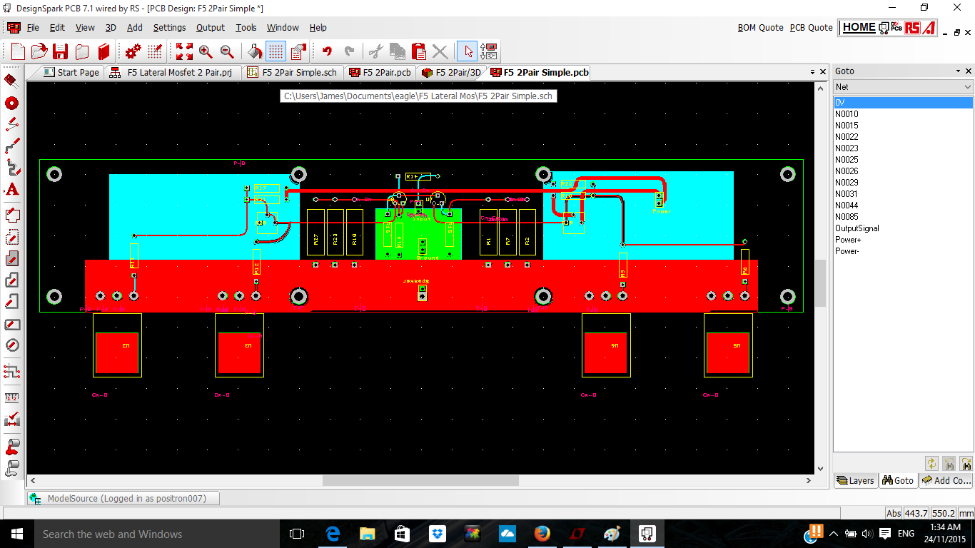
I'm making a few more changes tonight then it's going on the pcb mill tomorrow, and see what happens. Touch wood.
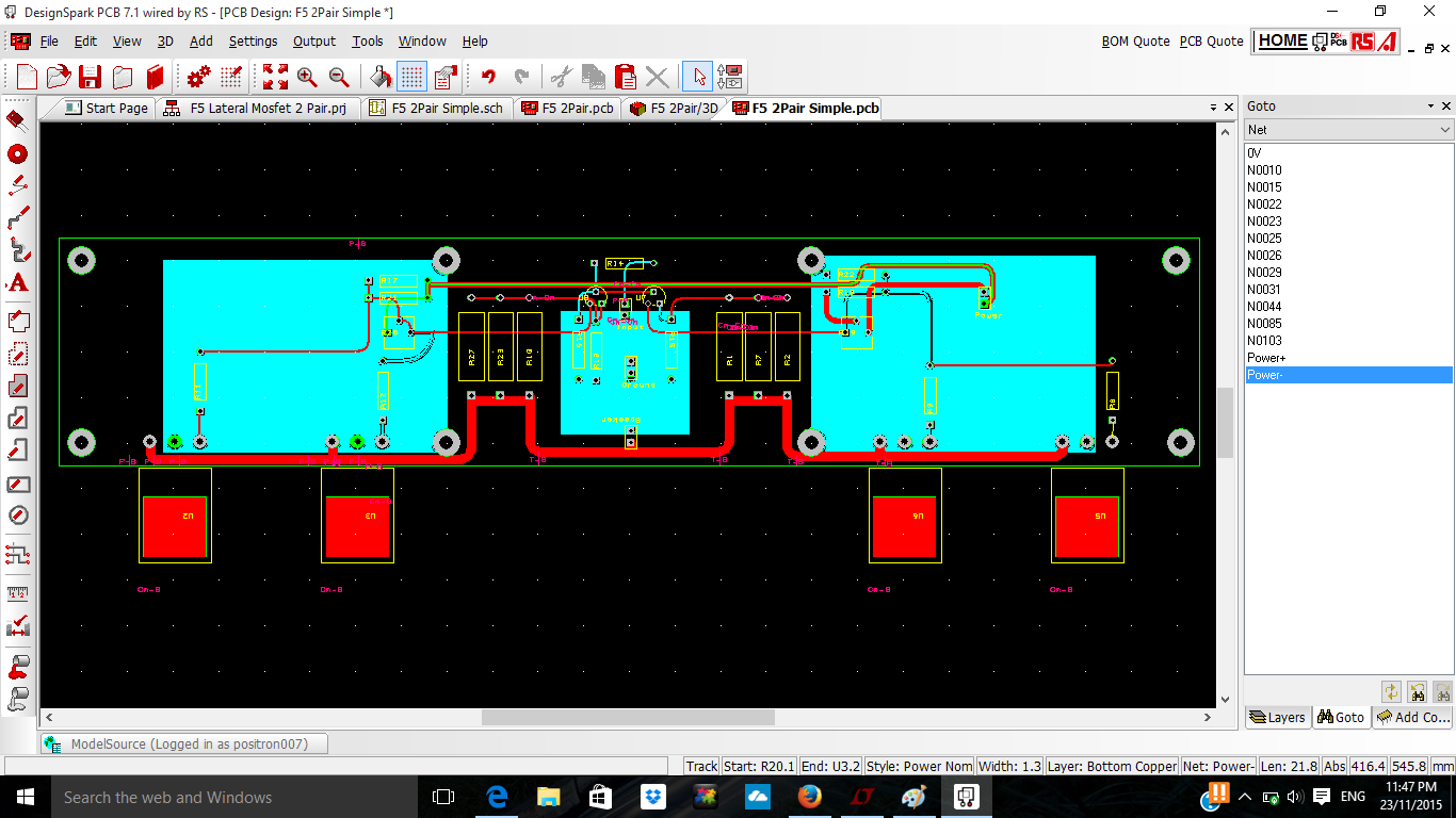
The speaker output rail at the bottom you have created is OK.
Make the same thing to the power input pours.
Move power input connector to the same place as you have the speaker output.
Move gate resistors down and to the right so that you have their tracks entering to the mosfet gates horizontally. That way they dont block your nice copper pours.
Turn JFET buffer transistors independently into such positions that the tracks into them are nice and straight, forget the extreme symmetry with them.
Try make everything as tiny and compact as possible and you should then get the loop areas automatically also as small as possible...
Move the feedback resistors closer to the speaker connector, their job is to monitor that terminal so make them do that.
same thing with the grounds. The ideal GND is at the speaker return.
Then when you think all is ready - redraw it 10 times more.
Last edited:
Ok. I'll get those things done, then I'm milling it. Need to just get something made that will work.
I'll keep revising it over time though.
I'll keep revising it over time though.
- Status
- Not open for further replies.
- Home
- Amplifiers
- Pass Labs
- Very First Attempt of PCB Layout Using Design Spark (Please Check)