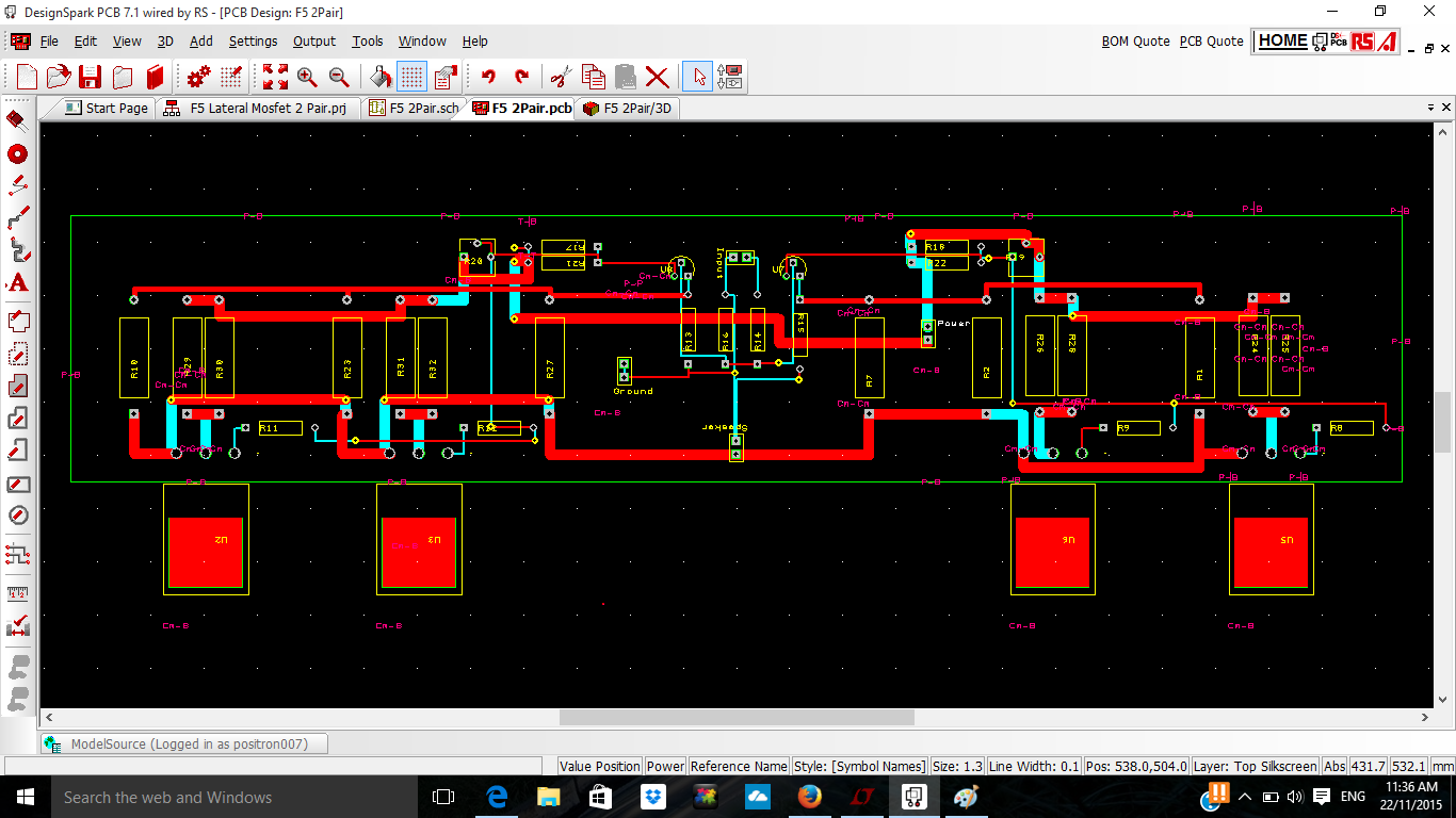
Going with 2 ounce copper (approx 75 micron)
Tracks are 2mm for power rails and signal out.
If all goes to plan, this will be the most Zen amp I have built to date.
The amp that the Caveman didn't build because he said it was too simple.
Issues
1) Not sure how to do ground plain
2) Not sure if I have made any fundamental errors with pcb layout.
3) Considering mover power input to new/better location
Last edited:
What is it? We would want a schematic to check against? I'm not familiar with your application but, I can tell you some stuff I've learned over the years.
I would say the most common thing overlooked is the actual component lead size (+ clearance) vs. the hole size in the layout. Also, the component lead spacing. It's good to actually have an example and bend the leads and measure. However, it is also good to think about other sizes that another diy'er might want to use. Especially Source Rs and other power Rs.
Another common mistake is mixing up bottom or top view with actual component orientation. Where you end up needing to insert a part upside down, which usually can't be accomplished. you can see this easily by looking at pin numbers from a top/component side view.
Also, the "ref des" needs to be visible with the component mounted.
Your pad diameters look a little small in most places. that will allow damage easily compared to more copper surrounding the pins.
Last edited:
Thanks. For the comments. I'll go check the pad sizes.
I'm not too concerned about the schematic, just worried about pcb layout rules etc.
If I post the schematic it will confuse the hell out of everyone. Hahaha. I am using IR parts in the schematic but wired them up incorrectly so that Lateral Mosfets will be correctly wired.
Resistor values are all wrong but package sizes and power rating are correct.
Input jfets are BC550/560 transistors cause they have same pinout as 2sk170/j74.
Basically the libraries are hopless. You have to think outside the box to make it work.
The amp is a simplified F5 with Lateral Mosfets, no thermistors required (0 tempco), no source resistors (however I have allowed for them, 2 per device for tweaking. I won't be using them.), no current limiting.
I have allowed for up to 3 pairs of feedback resistors per loop. I have added them locally near each device on pcb, not sure if that is the most ideal location (possibly better to put them in a centralised location near output pad).
I'll probably add cascode input later.
Edit: I already built something like this many years ago with IR devices and it worked perfectly but it always made me a bit nervous. The thing would take quite a while to stabilise.
With the laterals they bias up and remain rock solid almost immediately, so I thought it would be good to cut my teeth on PCB design with this circuit.
Last edited:
Avoid vias at power tracks/high current tracks. Jump between layers with the component leads if you must.
Put power tracks /high current tracks to the soldering side of the PCB.
Use all copper available to the high current tracks, meaning; use copper pours.
Or, you could try making one massive copper pour area (rail) for the speaker output to the top side (or bottom). And then similar very wide power rails to the opposite side, i.e. the bottom side (or top).
You are able to jump over these rails with the gate resistors, source resistors, and so on...
Avoid vias at power tracks/high current tracks. Jump between layers with the component leads if you must.
Put power tracks /high current tracks to the soldering side of the PCB.
Use all copper available to the high current tracks, meaning; use copper pours.
Or, you could try making one massive copper pour area (rail) for the speaker output to the top side (or bottom). And then similar very wide power rails to the opposite side, i.e. the bottom side (or top).
You are able to jump over these rails with the gate resistors, source resistors, and so on...
I will try to add as many of those ideas as possible.
Another reason why I like this one.
Nice 2nd Harmonic with virtually zero third and anything higher.
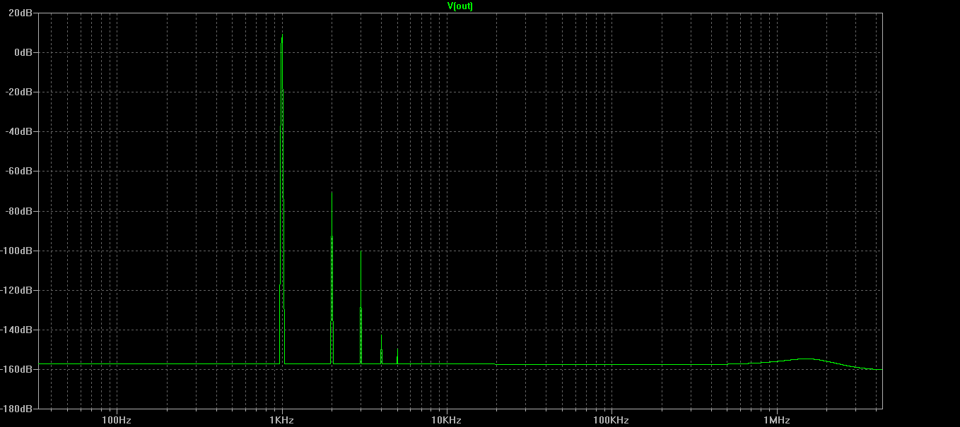
Nice 2nd Harmonic with virtually zero third and anything higher.
It is your first Layout?
Jean-Paul
First time using software, but have done quite a few point to point and a couple of etched boards just freely drawn.
About time I learn to use the software.
Last edited:
Don't cross lines allways for LF.
No vias as challenge.
70um copper --> vias and lines > 0.3mm.
Use copper pouring and don't forget layer copper balancing.
And much more...
My 2 cents, Jean-Paul
No vias as challenge.
70um copper --> vias and lines > 0.3mm.
Use copper pouring and don't forget layer copper balancing.
And much more...
My 2 cents, Jean-Paul
Don't cross lines allways for LF.
No vias as challenge.
70um copper --> vias and lines > 0.3mm.
Use copper pouring and don't forget layer copper balancing.
And much more...
My 2 cents, Jean-Paul
What is copper pouring? Like a mini ground plane?
What do you mean by layer copper balancing?
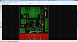
I think I am going to manually rout everything, part of the problem with software is it is so tempting to auto rout (as shown above) and assume the software will do a better job.
Forget autorouting! The component placement is dimensioning.
Copper pouring is copper plane. Use it for the power signals. LF + THT components --> Signal width > 0.6mm.
Copper balancing for manufacturing. The Process is starting with a complete 75um copper plane and you pay for that!
Copper pouring is copper plane. Use it for the power signals. LF + THT components --> Signal width > 0.6mm.
Copper balancing for manufacturing. The Process is starting with a complete 75um copper plane and you pay for that!
Forget autorouting! The component placement is dimensioning.
Copper pouring is copper plane. Use it for the power signals. LF + THT components --> Signal width > 0.6mm.
Copper balancing for manufacturing. The Process is starting with a complete 75um copper plane and you pay for that!
You still haven't explained what copper balancing is though 😕
The Balance between copper and copper free areas. More copper for better manufacturing processing!
Copper pouring is copper plane. !
Found this. RSTechSupport (Copper Pour, introduction and techniques). DesignSpark
I'll have to read through it later.
Thanks. For the comments. I'll go check the pad sizes.
I'm not too concerned about the schematic, just worried about pcb layout rules etc.
If I post the schematic it will confuse the hell out of everyone. Hahaha. I am using IR parts in the schematic but wired them up incorrectly so that Lateral Mosfets will be correctly wired.
Resistor values are all wrong but package sizes and power rating are correct.
Input jfets are BC550/560 transistors cause they have same pinout as 2sk170/j74.
Basically the libraries are hopless. You have to think outside the box to make it work.
The amp is a simplified F5 with Lateral Mosfets, no thermistors required (0 tempco), no source resistors (however I have allowed for them, 2 per device for tweaking. I won't be using them.), no current limiting.
I have allowed for up to 3 pairs of feedback resistors per loop. I have added them locally near each device on pcb, not sure if that is the most ideal location (possibly better to put them in a centralised location near output pad).
I'll probably add cascode input later.
Edit: I already built something like this many years ago with IR devices and it worked perfectly but it always made me a bit nervous. The thing would take quite a while to stabilise.
With the laterals they bias up and remain rock solid almost immediately, so I thought it would be good to cut my teeth on PCB design with this circuit.
You don't have to rely on the provided libraries, it is dead easy to create custom components in design spark.
Sent from my iPhone using Tapatalk
- Status
- Not open for further replies.
- Home
- Amplifiers
- Pass Labs
- Very First Attempt of PCB Layout Using Design Spark (Please Check)