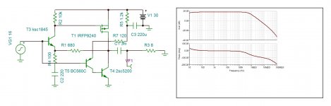
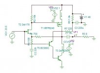
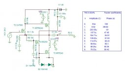
This is two amplifiers combined in push pull. The main power amp is made of open loop current amplifier T4,T5. The bias is adjusted by R5, 1.3A and the transconductance by R7. The second amplifier is also a transconductance with feedback to provide a low impedance output.
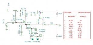
This is a quick feasibility circuit of 10w, with mosfet it is about 0.05% THD and the double with bjt version.
Hayk
Attachments
Last edited:
Nice and it does look very simple and sweet - another truly minimalist design but is there a reason not to use KSA992 or other low noise PNP for T5, the quasi-complement for T3?
Hi Ian, These are just "prova" circuits to have an idea what I can do with. The high light is the open loop current amp which needs high Hfe driver at 10ma.
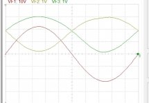
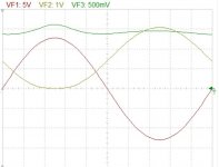
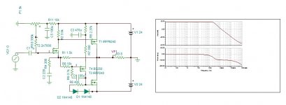
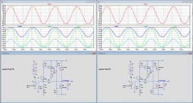
Here how it works. With 16 ohms load, the I amp works in SE where the V amp corrects the distortion.

With 8 ohms load, both V&I work equally.

With 50 ohm load the V swallows most of the I current.

I must review the current amp for more linearity.
Hayk
With 8 ohms load, both V&I work equally.
With 50 ohm load the V swallows most of the I current.
I must review the current amp for more linearity.
Hayk
Attachments

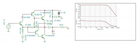
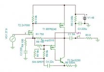
This is two switchable type of biasing. If the switch is closed, the I amp delivers half of required current for 8 ohm load. The amp is full class A.
If the switch is open, the I amp delivers all the current to 8 ohms load up to 9W, above it cuts off but the V amp remaining in class A all time fills in the blank.
By this the same amp can have two different sounds, of course an adjust instead of switch can make it variable to tune the sound.
Hayk
Attachments
Last edited:
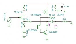
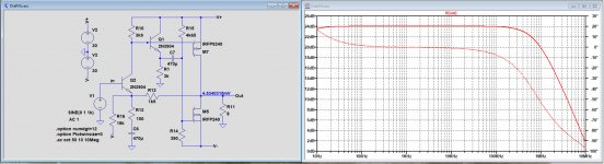
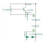
This is all Mosfet to have square law function. It requires only 1.15A bias for 30W 0.02% 1khz dissipating 55W. The C4 can be shorted and the bias readjusted once the value of R9 is determined.
Hayk
Attachments
Last edited:

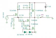
Hi Hans. Your amp is superb but not V/I. It needs thermal stability (two diodes glued upon the Nmosfet), and means to adjust the gain balance of the outputs (3.9k potentiometer instead of resistor).
Hi Hans. Your amp is superb but not V/I. It needs thermal stability (two diodes glued upon the Nmosfet), and means to adjust the gain balance of the outputs (3.9k potentiometer instead of resistor).
Hi Hayk,
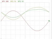
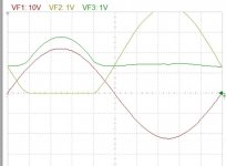
The 3k9 determines the voltage swing to the same amount for the positive and the negative MosFet, it's value has only effect on the loop gain and not on the balance of the outputs, see image below for 3K9 and 2K7.
Top graph is output voltage with below the current through the 8R resistor and both MosFets Drain currents. As you can see, it has no effect at all on balance and on Bias current.
The other thing is that although it may look a bit different, it is just as much a V/I as your design.
The lower MosFet acts as a modulated current source.
Connect R8 in your design to earth instead of to T2, and in my design disconnect C7, and both lower MosFets are constant current sources.
Now to modulate this current source in my case I take the T2's drain where I need no inverter and no gain, where you need an inverter with gain because T2's Source has a much lower voltage swing.
So both circuits are just as much V/I to my opinion.
It is just a raw design, so adding parts for thermal bias compensation would make sense.
Also adding an op-amp in front could further hit two birds with one stone.
As a servo to control the output offset voltage and at the same time by reducing the distortion substantially, and notice that R16 can be removed.
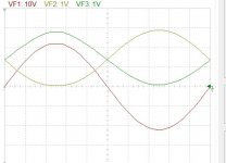
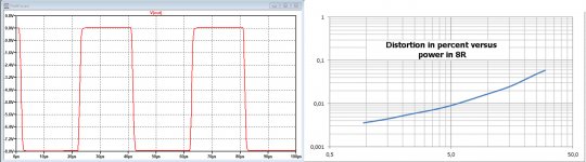
See the second image for a 1Khz 30Watt output.
Hans
P.S. I will try to spend some time hoping to understand why single and dual supply behave differently with your design.
Attachments

May be this way.

Or the emitter resistor to make potentiometer.
PSRR can be a problem.
By using the common inverting input transistor, you apply feedback also to the N mosfet which must remain open loop I amplfiier, this why the I amp to remain high impedance current source it needs it's own inverter. That is the I amp pours the current to the load, the V amp adjusts the distortion and Z load variations. As the V amp imposes its authority in SE, the amp behaves as SE as you see the harmonics.
Hayk
Attachments
Last edited:
Hayk,
About thermal compensation.
The Irfp mosfets have zero temp coefficients at around 5-6 Amp and a ever increasing positive temp coeff. at a decreasing drain current.
How did you come to the two compensation diodes, was this based on experiments or just an educated guess ?
Hans
About thermal compensation.
The Irfp mosfets have zero temp coefficients at around 5-6 Amp and a ever increasing positive temp coeff. at a decreasing drain current.
How did you come to the two compensation diodes, was this based on experiments or just an educated guess ?
Hans
The u of irfp240 is higher than the 9240, 4/3.3 at 1.33A according to the spice model. To balance the gains you need only to decrease the N mosfet drive. If they are not equal, the output cannot remain in class A at full power.
O.k. Thanks for the tip, but have you looked at the current graphs at full power in posting # 15.
The currents at 30Watt are almost perfectly equal, no need to adjust a thing.
Hans
The currents at 30Watt are almost perfectly equal, no need to adjust a thing.
Hans
- Home
- Amplifiers
- Solid State
- V/I class A Amplifier