ezkcdude said:Yeah. (Except I'm not using electrolytics on the regs, right?) By the way, what is the size of your board? I'm guessing it's quite a bit bigger than mine, because of those larger caps.
I've not compared directly, but I'd say mine is smaller as electrolytics have smaller size than other types for the capacitance.
ezkcdude said:At this point, I think I should really consider stopping further pcb development (except if there is a major issue) until I have the board physically in my hands. I will order it this week, and some parts from digikey, and maybe by next weekend, I can show a working result.
I think that's a good idea. The board is OK and if it suits your needs why chase round redeveloping things all the time. You get tired of it soon enough 😉
ezkcdude said:FastEddy, I tried adding the bridge option, but placement of the thire input connection is problematic.
If you want a bridge input as well FastEddy, you could always use my board 😀
Seriously, good work Dude and glad you have learnt something from my input and I'm flattered you chose my design as a base.
'lectrolitics v. poly v. mix of 'em
rich00boy: " ... but I'd say mine is smaller as electrolytics have smaller size than other types for the capacitance ..."
Interestingly if you use electrolitics (C1A, C1B, C2A, C2B, etc.) on ezkcdude 's board, if the "snubbing" capacitor (C9) across the head end of the bridge is made a decent sized plastic poly cap, the overall effect is the same as if all caps are poly ... or at least it is very, very hard to tell the difference.
Paralleling poly caps with electrolitics results in the best of both types, cost v. filtering, board real estate v. quality or the result ...
(I have done this with several real estate intensive / costs sensitive crossover networks ... paralleled new polys with old electrolitics and it works quite well. My rule of thumb = poly should be 2% to 5% of electrolitic capacity = 47 uF electro plus 2.2 uF poly = 49 uF =
😎 ... )
richie00boy said:If you want a bridge input as well FastEddy, you could always use my board 😀
Seriously, good work Dude and glad you have learnt something from my input and I'm flattered you chose my design as a base. [/B]
Thanks, for the kind words. By the way, I did add the bridge capability.
http://www.cellandtissue.com/ezdac/dual_supply_board.png
full wave v. half wave
Yes I see about the "double" diodes.
That gives the builder a whole bunch of possibile component mixes.
= two diodes, half wave, large caps = xformer secondary winding (or regulated wall wart) input to AC1 & AC2
= four diodes, full wave, somewhat smaller caps = xformer secondary winding input at AC1 & AC3 (and optional center tap xformer winding input at AC2)
= similar filtering quality = 🙂
Pulled the trigger last night. I should get the boards by Friday, along with a digikey order, so I can work on it over the weekend.
Update...Got the PCB today, and will start soldering tomorrow. One question I have is should I solder all the components from the bottom side? Also should the regulators be inserted "all the way" through the hole? If you click on the www button below, it will take you to my new webpage devoted to this and future DIY projects of mine.
Hi,
best to solder all components on one side.
Double sided PCBs could have components on both sides but you will find that only SMDs do that.
Fit and solder all the low profile components first. eg. resistors & diodes then medium height and finally the tall ones.
You may want to attach a spring clip heatsink to the semiconductor legs before soldering each leg.
Alternatively solder just one leg and move to another component and then come back to the second leg after allowing a cooling period.
The 'one pin then move on then come back' method is what I use for semiconductors. You can also align fiddly parts this way then come back and neaten the joint once the other joints have been made thus securing the component in place.
Thanks for the link as well 🙂
Thanks for the link as well 🙂
Solder one side only
AndrewT: "best to solder all components on one side. ... Double sided PCBs could have components on both sides but you will find that only SMDs do that. ... Fit and solder all the low profile components first. eg. resistors & diodes then medium height and finally the tall ones. ...
All the above works for me ...
AndrewT: " ... You may want to attach a spring clip heatsink to the semiconductor legs before soldering each leg. ... "
During soldering of IC's, To3's and other semiconductors this is a very very good idea ... Temproary heat sinks = Forcepts (roach clips?), small vise grips, locking pliers, those very large paper clips, even a bolt, nut & washers on a TO3 cans' tab, etc. ..... Especially when soldering with silver solder as the heat needed is greater (longer time with the iron) than lead based solder.
AbdrewT: " ... Alternatively solder just one leg and move to another component and then come back to the second leg after allowing a cooling period. ..." ... and ... richie00boy: " ... you can also align fiddly parts this way then come back and neaten the joint once the other joints have been made thus securing the component in place. ..."
You mentioned a link, but I don't see it ... please post again.
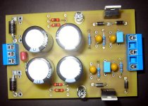
Success! It works on both +/- halves. I have it set up for half wave (D1,D2 populated) with 1000 uF, 63V caps for the smoothing. I'm using reg resistor of 3.01K and 332R, which is giving an output ~12.5V. I didn't have the right resistors for 15V, but that's o.k., since I have 2 boards left. I also put in the fuses. I'm excited! I was fully expecting it either a) not to work or b) to blow up in my face. So far neither has happened. Also, I noticed it takes several seconds for the voltage (current?) to discharge after I remove the inputs. I've always known that is supposed to happen, but it's fun to watch it on the scope.
Now, I need to figure out how to get some pictures. My digicam finally gave out the other day after many years (just my luck).
Now, I need to figure out how to get some pictures. My digicam finally gave out the other day after many years (just my luck).
Got a 'scope?
... to check the output and intermediate wave shapes (if any) = any noise riding on the output of feed line to the IC regulators, etc ...
... to check the output and intermediate wave shapes (if any) = any noise riding on the output of feed line to the IC regulators, etc ...
also you might ...
... experiment with replacing R1A (B, C) and or R2A (B, C) with coils ... inductors instead of resistors.
... experiment with replacing R1A (B, C) and or R2A (B, C) with coils ... inductors instead of resistors.
I wouldn't put inductors in, can be too problematic with resonances (you make an RLC circuit) and general instability of the reg chip. The circuit is pretty well filtered with the CRC network.
actually, ....
I believe that an industor at R1A (et al) would do the reverse of "resonate", since it would effectively become a very low pass filter, allowing only DC to pass ... L / C filter instead of R / C ...
I believe that an industor at R1A (et al) would do the reverse of "resonate", since it would effectively become a very low pass filter, allowing only DC to pass ... L / C filter instead of R / C ...
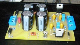
First Pic
My camera was o.k., but I needed a new flash card. Here's a pic. There will be more, but my camera battery needs to recharge. I'll do some more scoping tests tonight.
One thing you can probably tell from the pic is that there is not enough room for two 1N5403 diodes (i.e. D1',D2'). Oh, well. I can easily put more space and order new boards in the future.
Attachments
- Status
- Not open for further replies.
- Home
- Amplifiers
- Power Supplies
- Using unregulated AC wall wart