We are talking about how current send behaves.
Figure 5 explains what you are trying to convince everyone to be the case... but people have to try to apply what's written in the pdf, to a diamond (buffer) implementation of 844...
Nick
George, irrelevant to the discussion here !!!
.
Yeah, I don't give a rats a**e, you still misquoted me just a few posts back in reference to "your discussion", DON'T DO IT
Last edited:
the worst meeting we've had in ages.
After the meeting I deliberately went around and asked a number of the attendees how it went and it was very positive - Andrew especially as he would tell me the unvarnished truth. Talk to him and he will tell you something very different. So all I gotta ask George, what's your beef?
.
Figure 5 explains what you are trying to convince everyone to be the case... but people have to try to apply what's written in the pdf, to a diamond (buffer) implementation of 844...
Nick
No problem Nick. I got no beef with anything you or that that PDF says - in fact it looks like a good read and it is on a subject I am interesting in, maybe more than you realise as it has to do with a research project under way here in Sydney.
Also, everything I said is in total conformance with what's in that PDF read.
Somebody asked for a diagram or such - just takes a few moments to generate such a thing - but got one under way and later today I will post it.
In fact I hope you will find it interesting and have your comments, above all have a calm discussion about it. Trust me when I say that it conforms to completely conventional application - that is what makes it interesting. If it didn't, it would be a complete yawn, right?
So I am looking forward to post it and hope the discussion can be positive.
Cheers, Joe
.
After the meeting I deliberately went around and asked a number of the attendees how it went and it was very positive - Andrew especially as he would tell me the unvarnished truth. Talk to him and he will tell you something very different. So all I gotta ask George, what's your beef?
.
The usual is good/interesting write up's follow on SNA, and not a single one was done.
That is the barometer for how our meetings go.
As far any beef goes Joe none at all, I'll say it again "JUST DON'T MISS-QUOTE ME!!" And you still have not acknowledged it.
Cheers George
Last edited:
By the way, if some of you want to progress to more sophisticated and higher performance circuits with the AD844 check out the attached.
Not for the faint of heart but an excellent way to sharpen your circuit understanding skills!
I am indebted to Douglas Wadsworth for walking me through these many years ago!
Jan
Not for the faint of heart but an excellent way to sharpen your circuit understanding skills!
I am indebted to Douglas Wadsworth for walking me through these many years ago!
Jan
Attachments
The usual is good/interesting write up's follow on SNA, and not a single one was done.
That is the barometer for how our meetings go.
As far any beef goes Joe none at all, I'll say it again "JUST DON'T MISS-QUOTE ME!!" And you still have not acknowledged it.
Cheers George
 Down boy, relax.
First, I didn't misquote you. You did connect to Tz and you told me so. That's all. I never said that you did it for all eternity.
Two, I don't think you have understood the nature of the discussion at all.
No report? You mean no report yet (maybe I should have written a report?). Besides, it was Warren's meet - he asked me for help with only two days to go. So I helped - wasn't that good of me? Maybe next time won't bother. Alas...
Actually, it wasn't written because a certain person has been too busy. And it is not Sunday yet, so don't be too quick. It could be in your Inbox tonite?
Bad report? I have never heard anything that sounds really good at ASoN - so what? Set fire to the equipment or the hall? 😀
It seems only you and Elson have been unreasonably negative. Elson always sits in the back where everything sounds bad/worse. Were you by any chance sitting next to him? BTW, I give Elson heaps, but always in a good natured way - it took me three years telling him to use those US made JAN 12AT7WC's he had (hundreds of them).
https://www.youtube.com/watch?v=m00MQkYUNKo
I was buying heaps of him and telling him how good they were and finally he shows up at ASoN with amps using them and telling everybody they are his best effort yet - now he knows how good they are and he won't sell me any more. Should have kept my mouth shut (not really).
But that is what you call a moral victory. 😉
On top of that, he is now using them in amps he is building for Kiat with the Duntech name on them. But Kiat knows.
Sometime you don't get all the credit, but there is a God above who knows - IMHO.
Cheers, Joe
PS: On the topic of being misquoted, and I have Morris as my witness, you did indeed misquote me during the interval at ASoN - is it now my turn to get upset with you...? If not, why should you?
.
What a load misconscrewing and self promoting.
Ten hail Mary's and ten Our Fathers, for that post Joe.
PS: Your the one that bought God into it.
Cheers George
Ten hail Mary's and ten Our Fathers, for that post Joe.
PS: Your the one that bought God into it.
Cheers George
What a load misconscrewing and self promoting.
Ten hail Mary's and ten Our Fathers, for that post Joe.
PS: Your the one that bought God into it.
Cheers George
Now you are turning nasty George.
.
To the Moderator.
I do believe that post has stepped over the mark. Please, we don't need that.
I do believe that post has stepped over the mark. Please, we don't need that.
Hi,
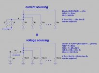
I assume what Joe meant was, that one can transform mathematically current steering into voltage steering or certain circuit structures into different circuit structures.
There are cases where such a transformation is useful, or even required.
In our case though I don´t think that it is of any positive use.
As current is what a current conveyor is all about.
We are not even interested in voltages in first place here!
And It is certailnly not required to get a grasp of the functioning of a current conveyor, but imho the opposite, because it rather results in misunderstandings and false views.
See first Diagram.
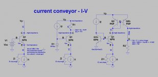
The second diagram describes the ´evolution´ of the current conveyor as used in the AD844, MAX435 and 436, and the OPA 660, 860 and 861.
As the DAC-Output is a current source the Q arises why not directly feed a I-V resistor and spare the hassle of building a active I-V converter stage alltogether.
Two resons:
- the ideal current source (cs) has a impedance value of infinity and a voltage compliance (allowed voltage level at their output) of infinity too.
a good practical cs shows values in the MOhm range.
All DACs outputs are rather low- to mid-ohmic, from a couple of hundreds ohms (ESS) to a couple of kOhms (ADI, BB).
So their outputs are far from beeing optimal cs.
- the typical Audio DACs feature protection Diodes that begin to conduct around ~300mV and are fully conducting for >600mV.
Therefore the I-V resistors value needs to be small enough that the voltage drop stays below ~300mV, otherwise the voltage co,pmliance of the DAC is surpassed and THD rises fast.
So, the question of using a I-V converter is about impedance matching and voltage compliance.
The left circuit shows the relationships in principle.
The Transistors Emitter is a low-impedance input, the lower the better.
Ideally the DAC (Cs) feeds into a 0Ohm impedance node.
Q1´s collector is a high-impedance output, that´s voltage compliance is restricted only by Q1´s maximum allowed collector-emitter voltage Vce.
We want the Emitter at least settling at a voltage potential within the DAC´s voltage compliance range, hence between +-300mV and we choose out of convinience 0V.
To make Q1 conduct its Base voltage must be sufficiently high, the Vbe.
So we supply Q1´s base with a voltage equalling the Vbe value.
The Transconductance is the neasure of the current variation through Q1 in relation to its Vbe.
The higher the transconductance the lower the Vbe change required for a certain current change.
So if we fix Vb at Vbe then the Emitter Potential will be nearly constant at 0V
One needs to add the low Emitter-input impedance times current through Q1 to the equation of the Emitter potential.
This also prooves the importance of E beeing a low-impedance node.
Neglecting the base current of Q1 here, the emitter current equals the collector current that flows towards the positive supply.
Besides the higher the transconductance of Q the lower its required Base current.
JFETs and MOSFETs are superior in this regard (at least within the Audio range), as they only feature tiny Gate-leakage currents.
The collector output impedance of Q1 can range from several tens of kOhms to nearly unmeasurable high.
The voltage compliance may be limited in the hundreds, if not thousands of Volts.
As such it resembles the ideal of a ccs much closer than the raw DAC output.
If now the collector current equals the DAC´s output current I1 then the collector will settle at Vsupply [Vp] minus DAC current [I1] times the collector Resistor value [R1]. (middle diagram).
The current I1 requires to have a dc-component I1dc so that V(C) settles at a idle value between Vp and V(B).
It´s common to choose V(C) around Vp/2, as that allows the most voltage excursion.
Factually You trim the values of I1dc and R1 depending on the desired V(C).
The Battery that supplied the V(B) for Q1 is replaced by a Diode, fed by a constant current source.
The voltage drop over the Diode (Vf) is similar to the Vbe of Q1 and if close coupled thermally it cancels the Tempco of Q1, stabilizing Q1´s emitter potential.
A MOSFET implementation is discussed at A New Take on the Classic Pass Labs D1 with an ESS DAc.
Or search for Jocko I-V for bipolar versions.
The simple Jocko bipolar I-V is already good for sufficiently low THD-values of up to -90dB at 0dBfs.
(most DataSheet speccs are for -3dBfs or even less signal level. We find OPAMP I-Vs no better than this simple circuit at 0dBfs, but with the hassle of global feedback and hundreds of parts forced by feedback to do something they wouldn´t do naturally 😉 )
As Q1 is used as a open-loop current buffer/impedance matcher it has a very high transit frequency --> it´s damn fast.
V(C) needs to be AC-coupled via a capacitor to a buffer stage.
As R1 is the I-V converting resistor and beeing connected to the supply line, the PSRR is 0.
Hence the supply lines need to be stiff and clean clean clean.
Diagram 3 now evolves further an one can see the similarities to the ´positive branch´ of the AD844.
Diode D1 is replaced by a transistor Q1b, which is the same type as Q1.
If one builds a discrete I-V stage Q1 and Q1b are preferrably matched Duals.
We also find a current mirror made from Q2 and Q2b at the collector of Q1.
At the collector of Q2b we find a exact mirror replica of I1, the current through Q1 and Q2.
R2 is the I-V conversion resistor and the same calculation apllies to R2 as has been done before to R1.
The advantage is that R2 is now referenced to 0V and the current mirror shields against the supply line.
Hence the PSRR is higher and the requirements regarding the supply are lower.
If the gnd contact potential of R2 is chosen at a defined negative voltage instead V(D) at idle may become 0V, thereby AC-coupling may be omitted with, allowing for DC-coupling to the following buffer stages.
V(C) settles at Vp minus the Vbe of Q2.
It varies only by a the change of Vbe(Q2) as reaction to the varying I1 through Q2 in the low mV range.
V(C) may be regarded constant, as it is non relevant for circuit analysis here anyway.
It only defines the upper limit that V(D) can swing to.
If Q2 were cascoded by another transistor to improve behaviour (raise impedance) the potential at node C is not exactly defined any more but can float (as the collector of the cascode transistor is not shortcut to its base like with Q2).
The potential of V(C) is irrelevant for the circuit functioning here.
The AD844 adds to this circuit basically only the complementary parts between the nodes E and D -and of course the integral buffer stage parts.
Circuit analysis of this circuit in the current domain is easy and straight forward.
There´s no transformation to the voltage domain required at all.
Instead it would only confuse and complicate things. 🙄
jauu
Calvin
ps: ... Einsteinian thinking ... why is it that his words about human foolishness come to my mind. 😀 (no pun intended)
I assume what Joe meant was, that one can transform mathematically current steering into voltage steering or certain circuit structures into different circuit structures.
There are cases where such a transformation is useful, or even required.
In our case though I don´t think that it is of any positive use.
As current is what a current conveyor is all about.
We are not even interested in voltages in first place here!
And It is certailnly not required to get a grasp of the functioning of a current conveyor, but imho the opposite, because it rather results in misunderstandings and false views.
See first Diagram.
The second diagram describes the ´evolution´ of the current conveyor as used in the AD844, MAX435 and 436, and the OPA 660, 860 and 861.
As the DAC-Output is a current source the Q arises why not directly feed a I-V resistor and spare the hassle of building a active I-V converter stage alltogether.
Two resons:
- the ideal current source (cs) has a impedance value of infinity and a voltage compliance (allowed voltage level at their output) of infinity too.
a good practical cs shows values in the MOhm range.
All DACs outputs are rather low- to mid-ohmic, from a couple of hundreds ohms (ESS) to a couple of kOhms (ADI, BB).
So their outputs are far from beeing optimal cs.
- the typical Audio DACs feature protection Diodes that begin to conduct around ~300mV and are fully conducting for >600mV.
Therefore the I-V resistors value needs to be small enough that the voltage drop stays below ~300mV, otherwise the voltage co,pmliance of the DAC is surpassed and THD rises fast.
So, the question of using a I-V converter is about impedance matching and voltage compliance.
The left circuit shows the relationships in principle.
The Transistors Emitter is a low-impedance input, the lower the better.
Ideally the DAC (Cs) feeds into a 0Ohm impedance node.
Q1´s collector is a high-impedance output, that´s voltage compliance is restricted only by Q1´s maximum allowed collector-emitter voltage Vce.
We want the Emitter at least settling at a voltage potential within the DAC´s voltage compliance range, hence between +-300mV and we choose out of convinience 0V.
To make Q1 conduct its Base voltage must be sufficiently high, the Vbe.
So we supply Q1´s base with a voltage equalling the Vbe value.
The Transconductance is the neasure of the current variation through Q1 in relation to its Vbe.
The higher the transconductance the lower the Vbe change required for a certain current change.
So if we fix Vb at Vbe then the Emitter Potential will be nearly constant at 0V
One needs to add the low Emitter-input impedance times current through Q1 to the equation of the Emitter potential.
This also prooves the importance of E beeing a low-impedance node.
Neglecting the base current of Q1 here, the emitter current equals the collector current that flows towards the positive supply.
Besides the higher the transconductance of Q the lower its required Base current.
JFETs and MOSFETs are superior in this regard (at least within the Audio range), as they only feature tiny Gate-leakage currents.
The collector output impedance of Q1 can range from several tens of kOhms to nearly unmeasurable high.
The voltage compliance may be limited in the hundreds, if not thousands of Volts.
As such it resembles the ideal of a ccs much closer than the raw DAC output.
If now the collector current equals the DAC´s output current I1 then the collector will settle at Vsupply [Vp] minus DAC current [I1] times the collector Resistor value [R1]. (middle diagram).
The current I1 requires to have a dc-component I1dc so that V(C) settles at a idle value between Vp and V(B).
It´s common to choose V(C) around Vp/2, as that allows the most voltage excursion.
Factually You trim the values of I1dc and R1 depending on the desired V(C).
The Battery that supplied the V(B) for Q1 is replaced by a Diode, fed by a constant current source.
The voltage drop over the Diode (Vf) is similar to the Vbe of Q1 and if close coupled thermally it cancels the Tempco of Q1, stabilizing Q1´s emitter potential.
A MOSFET implementation is discussed at A New Take on the Classic Pass Labs D1 with an ESS DAc.
Or search for Jocko I-V for bipolar versions.
The simple Jocko bipolar I-V is already good for sufficiently low THD-values of up to -90dB at 0dBfs.
(most DataSheet speccs are for -3dBfs or even less signal level. We find OPAMP I-Vs no better than this simple circuit at 0dBfs, but with the hassle of global feedback and hundreds of parts forced by feedback to do something they wouldn´t do naturally 😉 )
As Q1 is used as a open-loop current buffer/impedance matcher it has a very high transit frequency --> it´s damn fast.
V(C) needs to be AC-coupled via a capacitor to a buffer stage.
As R1 is the I-V converting resistor and beeing connected to the supply line, the PSRR is 0.
Hence the supply lines need to be stiff and clean clean clean.
Diagram 3 now evolves further an one can see the similarities to the ´positive branch´ of the AD844.
Diode D1 is replaced by a transistor Q1b, which is the same type as Q1.
If one builds a discrete I-V stage Q1 and Q1b are preferrably matched Duals.
We also find a current mirror made from Q2 and Q2b at the collector of Q1.
At the collector of Q2b we find a exact mirror replica of I1, the current through Q1 and Q2.
R2 is the I-V conversion resistor and the same calculation apllies to R2 as has been done before to R1.
The advantage is that R2 is now referenced to 0V and the current mirror shields against the supply line.
Hence the PSRR is higher and the requirements regarding the supply are lower.
If the gnd contact potential of R2 is chosen at a defined negative voltage instead V(D) at idle may become 0V, thereby AC-coupling may be omitted with, allowing for DC-coupling to the following buffer stages.
V(C) settles at Vp minus the Vbe of Q2.
It varies only by a the change of Vbe(Q2) as reaction to the varying I1 through Q2 in the low mV range.
V(C) may be regarded constant, as it is non relevant for circuit analysis here anyway.
It only defines the upper limit that V(D) can swing to.
If Q2 were cascoded by another transistor to improve behaviour (raise impedance) the potential at node C is not exactly defined any more but can float (as the collector of the cascode transistor is not shortcut to its base like with Q2).
The potential of V(C) is irrelevant for the circuit functioning here.
The AD844 adds to this circuit basically only the complementary parts between the nodes E and D -and of course the integral buffer stage parts.
Circuit analysis of this circuit in the current domain is easy and straight forward.
There´s no transformation to the voltage domain required at all.
Instead it would only confuse and complicate things. 🙄
jauu
Calvin
ps: ... Einsteinian thinking ... why is it that his words about human foolishness come to my mind. 😀 (no pun intended)
Attachments
Last edited:
How does this setup work with a really high DC offset? Looks like most of the talk about DC offset nulling with the 2SK170 and using 20k pot between pins 1 and 8 is about millivolts. I am thinking about using this on a TDA1545A that has a DC offset of about 3.3V when running from 5V supply (it is a single supply DAC with the reference voltage created by a resistor divider). The current from the DAC is 1mA so it is similar to much discussed PCM1704 here.
Hi,
I assume what Joe meant was, that one can transform mathematically current steering into voltage steering or certain circuit structures into different circuit structures.
There are cases where such a transformation is useful, or even required.
In our case though I don´t think that it is of any positive use.
Hi Calvin
You sound like a more measured voice and I welcome that.
So what is this all about?
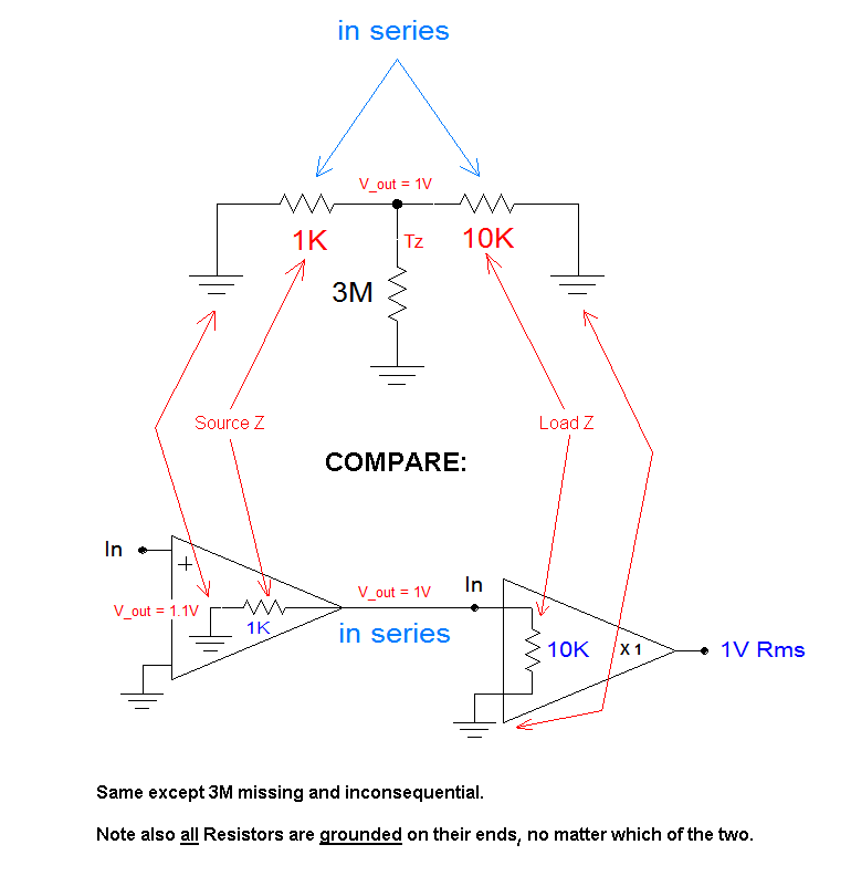
Wow! I made an off the cuff remark where two resistors can look to be physically in parallel, and yet where they are joined by a high impedance current source (I believe you said 3M) are effectively in series and where they actually act as a voltage divider.
Reason is that the high Z source becomes invisible to the lower values. Indeed in that triangular join the current source can be seen as a reflector - think about it, that can have some interesting uses.
Now going by your lengthy and extemporary journey, I now fairly believe that you knew what I meant, and what was no more than a running remark turned into a torrent of abuse where I was accused of espousing snake oil.
Not so.
So, what eally happened here?
Scott Wurcer turns up and for some reason Scott, whom I have never met and have nothing against, seems to have an agenda against me - because of an earlier topic called the "Rasmussen Effect" and that now seems to colour everything I say or do in his eyes. BTW, it was NOT coined by me here in Sydney, but by a guy in the US.
George OTH seems to have some kind of inferiority complex towards me and I cannot fathom why. Don't care. Circa 1995 George phoned me about getting a Rogue tube amplifier to sound better and over a number of phone calls that was all nice and cordial, I guided him through a number of steps on how to make the Rogue sound better, basic stuff like converting into triodes, get rid of electro-cathode resistor in the feedback path, stuff like that. He reported back as working nicely. It was only some time later we met each other in the flesh. Now George behaves one way towards me when we are by ourselves, and a completely different way when other people are around, it turns into a competition. What's going on? What's that about?
I really don't need this personal stuff - I have had a great week and nothing is going to take the smile of my face. 😀
---
OK, somebody demanded that I should come up with some "supporting material, i.e. pictures" diagram that would support my "claim" (which it is not, it was an observation and no more), so fair enough, I did and will post them.
I think you, Calvin, would be able to make perfect sense of it and put this to bed. It need not go on beyond that or it's just ridiculous.
This not snake oil:
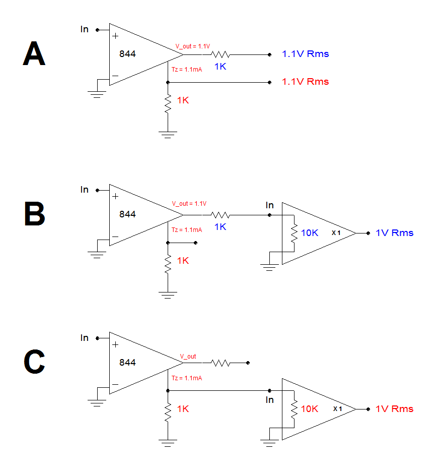
The above C can also be presented as:
Really, as I stated earlier, "Nothing I have said here is earth-shattering!"
What an over-reaction !!!
And certainly no snake oil - good grief.
Hi,
In our case though I don´t think that it is of any positive use.
I am not so sure about that. There is a huge amount to be learned - it has let me be open to a number of 'tricks' that I would not have otherwise been receptive to. Like hiding the centre-tap of a transformer can have interesting benefits and open up useful techniques. It is also useful in understanding loudspeaker design - and where next?
Who is to say what is in and what is out?
How about inserting an RIAA design at Tz? Does that get any juices going? Think about it. An RIAA with no current phase shift.
Hi,
And It is certailnly not required to get a grasp of the functioning of a current conveyor, but imho the opposite, because it rather results in misunderstandings and false views.
An element of truth there. Explain to novices in terms of a "voltage" model and what the see on a scope, that is easy and fairly intuitive. Vertical is volts, lateral is time, X-Y. Easy. But explain how voltage can be derived from current and their eyes glazes over. Many things become the opposite, like looking at a negative film. This is where I made a simple remark and observation, that when dealing with current, things can be different, where two resistors that are physically in parallel can also be seen as being in series, and even be observed to act effectively as a voltage divider.
I believe that you know exactly what I mean. Hope I have not misjudged that.
The world is a wonderful place to be - what a playground - and what we see often depends on what we look for and how we look at it.
Cheers, Joe
Last edited:
Joe, your last pic is definitely NOT in series - two resistors, connected together at both ends - that the definition of parallel!
A voltage divider?? Both resistor have exactly the same voltage - they are connected on both sides! You really have to read up on this basic stuff!
Don't tell me that you mean 'drawn in series but electrically parallel' - that's even more daft!
Re: feeling hurt: maybe you should take out some time and reflect on WHY lots of people seemingly have a gripe with you?
Jan
Last edited:
How about inserting an RIAA design at Tz? Does that get any juices going? Think about it. An RIAA with no current phase shift.
Like you said, nothing new here...
And what, no current phase shift?? Do you realise a RIAA network is full of caps and causes all kinds of phase shift; HAS to because amplitude response shaping is accompanied by phase shift shaping?
Jan
Hi,
commenting on Your diagrams.
Diagramm B: You charmingly missed to note that the current value through the 1k/10k path reduces to 100µA.
As the AD844´s Buffer output is just 15Ohms the output voltage without the -not at all required- 1k resistor would rise to 1.098V and the current would be 109.8µA.
So current values at TZ and the Buffer output differ by appr. a factor of 10 -as expected.
In Diagram C: You also didn´t note the currents through the 1k and 10k resistor.
The 1mA through the 1k and the 100µA through the 10k result in equal voltage drops, hence in settles at 1V.
To justify Your idea -I still don´t really get it though- and to proove the results You add a not at all necessary part ..... well if that makes Your understanding easier, so be it.
Last Diagram: Which of the above diagrams shall it refer to?
As representation of Diagram B, taking the signal from the AD844s buffer output, we need to omit with the 3M resistor alltogether and the signal is fed from the left gnd into the 1k.
And as written before, the 1k isn´t necessary at all and could be replaced at best by the 15R internal open-loop resistance of the buffer part.
As representation for Diagram C a ideal CCS connected between the common node and gnd is required, hence the three resistors appear all in parallel to each other and the CCS.
So the points where Voltage resp. current are fed into theis simplified circuit diagram differ.
What do You want to compare on such a faulty basis? 🙄
I´d rather stick to the common straight forward analysis.😛
jauu
Calvin
commenting on Your diagrams.
Diagramm B: You charmingly missed to note that the current value through the 1k/10k path reduces to 100µA.
As the AD844´s Buffer output is just 15Ohms the output voltage without the -not at all required- 1k resistor would rise to 1.098V and the current would be 109.8µA.
So current values at TZ and the Buffer output differ by appr. a factor of 10 -as expected.
In Diagram C: You also didn´t note the currents through the 1k and 10k resistor.
The 1mA through the 1k and the 100µA through the 10k result in equal voltage drops, hence in settles at 1V.
To justify Your idea -I still don´t really get it though- and to proove the results You add a not at all necessary part ..... well if that makes Your understanding easier, so be it.
Last Diagram: Which of the above diagrams shall it refer to?
As representation of Diagram B, taking the signal from the AD844s buffer output, we need to omit with the 3M resistor alltogether and the signal is fed from the left gnd into the 1k.
And as written before, the 1k isn´t necessary at all and could be replaced at best by the 15R internal open-loop resistance of the buffer part.
As representation for Diagram C a ideal CCS connected between the common node and gnd is required, hence the three resistors appear all in parallel to each other and the CCS.
So the points where Voltage resp. current are fed into theis simplified circuit diagram differ.
What do You want to compare on such a faulty basis? 🙄
I´d rather stick to the common straight forward analysis.😛
Well just hop over to the Paradise-Phono thread, or Alex Nikitin´s design for Creek, or the Air-Phono as examples of current fed RIAA.How about inserting an RIAA design at Tz...
jauu
Calvin
Like you said, nothing new here...
And what, no current phase shift?? Do you realise a RIAA network is full of caps and causes all kinds of phase shift; HAS to because amplitude response shaping is accompanied by phase shift shaping?
Jan
Yes, I was um and ah'ing about that too. Current source can only produce current with a zero degree current phase angle.
Hi,
ahemm You are not really trying to tell us that a real current (0° phase shift) fed into a complex impedance (phase shift, example: RIAA) results in real voltage (0° phase shift) are You???
jauu
Calvin
ahemm You are not really trying to tell us that a real current (0° phase shift) fed into a complex impedance (phase shift, example: RIAA) results in real voltage (0° phase shift) are You???
jauu
Calvin
'Phase shift' cannot exist in itself, it is always with reference to something else, just as 'voltage' is always in ref to something else. A point in a circuit cannot have 'a voltage'- it can only have a voltage in reference to ground or supply or whatever.
So any source has always zero phase shift to itself - that's a nobrainer. You can only sensible speak about phase shift of a current with respect to another current or voltage, and of course any source can have any phase shift with reference to another voltage or current.
Jan
So any source has always zero phase shift to itself - that's a nobrainer. You can only sensible speak about phase shift of a current with respect to another current or voltage, and of course any source can have any phase shift with reference to another voltage or current.
Jan
Hi,
commenting on Your diagrams.
Diagramm B...charmingly
Whoa!!!
I could have put OPA660 or even OPA860 (very low Z).
I have even measured samples of the output impedance of 844s and it's not 150R, not even near it.
In the diagram, the 1K is the defined output impedance - I am surprised you should nit-pick such a thing.
Don't over-analyse it - no need to - it was just to illustrate a point and no need for anything more. None of this 'charmingly' stuff.
I made the point. Others I have shown this too had no difficulty, so that's all there is to it.
I can certainly produce full working schematics and then it would be fair and proper to subject to the analysis you seem to attempt. It is hardly appropriate here.
Last Diagram: Which of the above diagrams shall it refer to?
Calvin, it clearly said C:
Hi,
Well just hop over to the Paradise-Phono thread, or Alex Nikitin´s design for Creek, or the Air-Phono as examples of current fed RIAA.
I have already done that at least ten years ago.
Are you aware of anybody done it with AD844? I think I remember somebody who did - a fellow Dane like me. Somebody whose name even George would recognise. Lars Clausen.
-----
I still make the point and I stand by it - that the representative diagrams I presented shows clearly how those two resistors behave - this is the nature of current as opposed to voltage - I see nobody here 'destroying' that basic observation.
If somebody don't want to see it, then that is their prerogative - but others have not had that problem.
And to those who look, this is basic.
Cheers, Joe
PS: I am reminded of the saying "I can't see the Forrest for all those trees."
.
Last edited:
- Home
- Source & Line
- Digital Line Level
- Using the AD844 as an I/V