john curl said:Please go to page 14 of the HK manual. That wasn't so hard, was it?
So you were referring to the phono stage instead of the line stage?
Ok, graphic's been updated.
se
john curl said:Bob, have you ever looked at the schematic of the Harmon Kardon Citation 17s preamp? You should check it out.
Close, but they didn't fully get it. That circuit does not provide a true current source load, although it gets the impedance higher than many. Had they provided the base bias of the differential current sources by summing to common mode after the emitter followers, then they would have had the circuit I used.
Cheers,
Bob
Steve Eddy said:Thanks, Andy.
And to make it easier for others to reference in this thread, here's the schematic in question (assuming John wasn't taking about the input of the phono stage).
An externally hosted image should be here but it was not working when we last tested it.
se
Thanks, Steve!
Bob
Hi Bob,
--- Do you have a schematic of that Hitachi circuit? I don't think I'm familiar with it, but would certainly be interested in seeing any earlier references to circuits like the one I used.---
Maybe the generic term I used had puzzled you as you are very familiar with this kind of circuit. It was called "Hitachi" because it started to be often used after an application note published by the japanese manufacturer at the release of their Mosfets : it consists of two differential stages of opposite polarity, the second one being loaded by a current mirror. Here is an evolution of the initial circuit :
Attachments
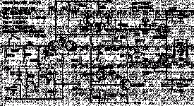
The Citation 17 circuit is over 30 years old. I first saw it when I worked with the designer of the circuit at HK in 1977. I was impressed by the dual active loading, at the time, so I remembered it well enough to bring it up, today.
The Hitachi circuit is based on the Marantz 14 power amp that is almost 10 years older than the HK circuit. The biggest difference was that mosfets were not invented yet. This does not change the topology, however.
You will also find an example of the 'Hitachi' topology in the Levinson JC-2 phono stage circuit, developed in 1973. The largest difference is the use of jfets on both the input and the output stage.
forr said:Hi Bob,
--- Do you have a schematic of that Hitachi circuit? I don't think I'm familiar with it, but would certainly be interested in seeing any earlier references to circuits like the one I used.---
Maybe the generic term I used had puzzled you as you are very familiar with this kind of circuit. It was called "Hitachi" because it started to be often used after an application note published by the japanese manufacturer at the release of their Mosfets : it consists of two differential stages of opposite polarity, the second one being loaded by a current mirror. Here is an evolution of the initial circuit :
Thanks for bringing that to my attention. That's a pretty obvious and generic topology; its the way just about anybody would start out to arrive at a complementary VAS starting with a single differential input stage. I'm a little surprized it is called the "Hitachi" topology.
The key thing that the circuit I used brings to the table is the differential current source load that buffers the signal and provides common-mode rejection at the same time. Although I don't recall seeing it anywhere else, I'd guess that someone else probably first used it before me, perhaps inside an IC op amp.
Thanks,
Bob
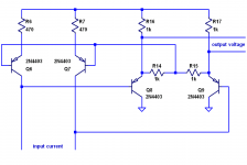
Differential Current Source Load
For the convenience of all, below is the schematic of the 4-transistor differential current source load that I have been talking about. It is really quite a simple circuit, but does a lot with only four transistors. Q6 and Q7 are the actual current source loads. Q8 and Q9 serve to buffer the outputs, effectively acting as Darlington transistors for the following stage (which would typically be a differential pair). At the same time, the summed buffered output of Q8 and Q9 biases the bases of the current sources. This effectively causes the common mode input impedance of the circuit to be low, aiding in overall common-mode rejection.
Note that the output rails are conveniently below the positive rail by one Vbe plus the drop across R6/R7. This conveniently sets up the tail current for a following differential stage that merely uses a resistor in its tail. The idle current in the second differential pair will be set to a scaled value of the tail current of the input differential pair that drives this differential current source load.
Bob
Attachments
john curl said:Now I am going to give you fellow designers a real challenge. Did you know that Doug Self is right that bipolar transistor differential pairs actually generate LESS harmonic distortion than jfet differential pairs? There is an IEEE paper on the subject. Study that, and it would appear that you should not use differential fet pairs in any configuration.
This is interresting! And no one picked up the thread!
From Chapter 4 in Douglas Self's book "Audio Power AMplifier Design Handbook", he himself writes:
"BJTs vs FETs for the input stage
At every stage in the design of an amplifier, it is perhaps wise to consider whether BJTs or FETs are the best devices for the job. I may as well sayat once that the predictable Vbe/Ic relationship and much higher transconductance of the bipolar transistor make it, in my opinion, the best choice for all three stages of a generic power amplifier. To quickly summarise the position:
Advantages of the FET input stage
There is no base current with FETs, so this is eliminated as a source of DC offset errors. However, it is wise to bear in mind that FET gate leakage currents increase very rapidly with temperature, and under some circumstances may need to be allowed for.
Disadvantages of FET input stage
1 The undegenerated transconductance is low compared with BJTs. There is much less scope for linearising the input stage by adding degeneration in the form of source resistors, and so an FET input stage will be very nonlinear compared with a BJT version degenerated to give the same low transconductance,
2 the Vgs offset spreads will be high. Having examined many different amplifier designs, it seems that in practice it is essential to use dual FETs, which are relatively very expensive and not always easy to obtain. Even then, the Vgs mismatch will probably be greater than Vbe mismatch in a pair of cheap discrete BJTs; for example the 2N5912 N-channel dual FET has a specified maximum Vgs mismatch of 15mV. In contrast the Vbe mismatches of BJTs, especially those taken from the same batch (which is the norm in production) will be much lower, at about 2–3mV, and usually negligible compared with DC offset caused by unbalanced base currents,
3 the noise performance will be inferior if the amplifier is being driven from a low-impedance source, say 5 kohm or less. This is almost always the case."
I do not have the IEEE paper, but I looked up in his book, and this quote is all I found after a very rapid search.
I would very much like to know why on Earth you all use JFETs then ;-)
Has it something to do with higher harmonics decaying in a nicer manner with JFETs than bipolars, even if the THD as such is higher?
Regds
Rolv-Karsten
Actually the complementary differential fet approach does not necessarily have as much a problem as a single differential fet approach does, and it is self biasing, lower noise, (Doug Self is really off base on this one) and more linear (when higher order distortion is weighted properly) than a differential input stage.
john curl said:Actually the complementary differential fet approach does not necessarily have as much a problem as a single differential fet approach does, and it is self biasing, lower noise, (Doug Self is really off base on this one) and more linear (when higher order distortion is weighted properly).
Yes, thank you. It seems Self believes in single differential pairs. Many other British amplifiers use the same (and Bob Cordell's amp in JAES (1985 or so?)) approach, single diff pair, often PNPs. (Or maybe it is only the power amplifiers proposed in the "Wireless World" magazine.)
Regds
Rolv-Karsten
It is the result that counts. And I do not know superbly sounding Cambridge Audio, usually opposite is truth 😉
We invented the complementary differential input stage here in the USA in the 1960's. American engineers had easy access of complementary small signal devices, even as matched pairs, in the late 1960's through Motorola and other manufacturers.
In 1972, I showed Bob Stuart of Meridian the complementary differential transistor pair, and he started to use it immediately.
In 1972, I showed Bob Stuart of Meridian the complementary differential transistor pair, and he started to use it immediately.
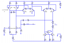
Single-Pair Differential Input and VAS Stage
For your convenience, below I show the basic schematic of the input stage and VAS that I use, devoid of the cascodes. You can see that it is really quite simple. Just a FET input differential pair loaded by the differential current source load. That is followed by a VAS differential pair loaded by a current mirror.
This circuit does not require one to hunt around for decent p-channel complement pairs.
Cheers,
Bob
Attachments
Low open loop bandwith is my greates concern. Noise injection from the active load is another. This could be a problem if this topology was used for a phono or microphone input.
john curl said:Low open loop bandwith is my greates concern. Noise injection from the active load is another. This could be a problem if this topology was used for a phono or microphone input.
This topology is open-loop-bandwidth-agnostic. Those who think that wide open loop bandwidth is necessary can easily arrange for this topology to have just as wide open-loop bandwidth as any other. A single resistor across the collectors of the input pair will do it, and linearity will still be extremely good.
As for S/N, this circuit delivered an A-weighted S/N of 108 dB ref 1W at 8 ohms in my amplifier. The JC-1 delivers an A-weighted S/N of only 88 dB.
Cheers,
Bob
There are IEEE papers and and MAT02 matched bipolar-pair application notes that show very good SNR for bipolar cascodes.
Are there secondary sonic issues with the cascode and folded cascode topology?
Which input topology would be best for a power amp with no global feedback? Perhaps also using On-Semi Thermal Track bipolars in the T-output with Hawksford error correction.
Are there secondary sonic issues with the cascode and folded cascode topology?
Which input topology would be best for a power amp with no global feedback? Perhaps also using On-Semi Thermal Track bipolars in the T-output with Hawksford error correction.
Attachments
LineSource said:Which input topology would be best for a power amp with no global feedback?
This is along the lines of what I'd been thinking about today.
The basic Lin topology is built up from input, voltage amplification, and output stages. And although the voltage amplification stage is called what it is, all of these input stages also provide voltage amplification.
It would seem that the only reason for this is to build up a lot of excess voltage gain between the input and the output with the expectation that there will be a global feedback loop tying everything together and subsequently bringing the gain down to what you actually need in the end.
If that's the case, and if one were interested in a design which had no global feedback loop, it would therefore seem that there would be no particular need for the input stage to provide any voltage gain.
Yes?
se
Steve Eddy said:
If one were interested in a design which had no global feedback loop, it would therefore seem that there would be no particular need for the input stage to provide any voltage gain.
Yes?
se
Charles Hansen mentioned that all the voltage gain in his latest amp was in the input stage. The VAS and output stages shifted levels and amplified current. This is the type of no global feedback designs I have been playing with.
- Status
- Not open for further replies.
- Home
- Amplifiers
- Solid State
- Unipolar vs complementary input stage