For noise spectrum measurements like PS, references, batteries etc.
Gain 60 dB, bandwidth 4 Hz- 500 kHz (GBW - 500 MHz), noise below 400 pV/sqrt(Hz).
Inspired by:
http://www.dicks-website.eu/low_noise_amp_part3/part3.html
https://www.diyaudio.com/community/threads/ad8428-low-noise-preamplifier.407270/page-3#post-7910879
https://keith-snook.info/transistor-noise-and-rbb.html
Choices made.
-no extra large electrolytics, so no DC NFB, just auto bias;
-single power line, common LM317 regulated (noisy) power source;
-no expensive electronic components.
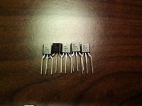
Transistors:
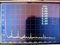
Results:
-120 coresponds 1 nV.
Schematics:
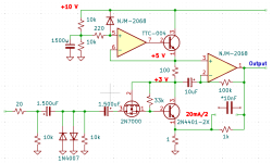
Circuits description:
TTC-004 is a denoiser/ PS ripple suppressor.
2N7000 is active input protection - saves BJT during input conection/ disconnection
overstress.
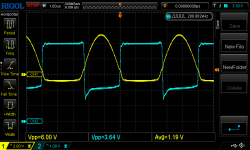
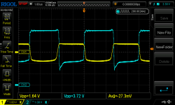
Real crash test of input protection:
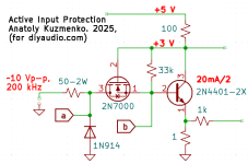
yellow - base voltage, blue - collector.
Gain 60 dB, bandwidth 4 Hz- 500 kHz (GBW - 500 MHz), noise below 400 pV/sqrt(Hz).
Inspired by:
http://www.dicks-website.eu/low_noise_amp_part3/part3.html
https://www.diyaudio.com/community/threads/ad8428-low-noise-preamplifier.407270/page-3#post-7910879
https://keith-snook.info/transistor-noise-and-rbb.html
Choices made.
-no extra large electrolytics, so no DC NFB, just auto bias;
-single power line, common LM317 regulated (noisy) power source;
-no expensive electronic components.
Transistors:

Results:
-120 coresponds 1 nV.

Schematics:

Circuits description:
TTC-004 is a denoiser/ PS ripple suppressor.
2N7000 is active input protection - saves BJT during input conection/ disconnection
overstress.
Real crash test of input protection:

yellow - base voltage, blue - collector.


Thanks for sharing your design! The protection circuit is very clever. I'm impressed at the noise performance you were able to achieve.
I'm not familiar with the instrument you are using to generate the bode plot and am not sure how to read it. Does the 1/f noise limit the lower end of the bandwidth, or is that calculated based on your various RC time constants?
My quick math says that the 20 ohm protection resistor on the input would contribute 0.580 nV/sqrt(Hz) of noise right off the bat. Did you need to short it to achieve the 400pV/sqrt(Hz) figure?
Project in progress, running on breadboard at this time.I'm not familiar with the instrument you are using to generate the bode plot and am not sure how to read it. Does the 1/f noise limit the lower end of the bandwidth, or is that calculated based on your various RC time constants?
Instrument:
In the mid-scale error about +-1 dB. Verified by Rigol 1022 SG, two steps divider /100dB to get 10 & 100 nV markers.
I've build another SA ads131m04 based, 4 channel and log freq. chart starting from 0.1Hz on the left. But not using for now, since fft-32k takes about 2 min to update screen, not any good if doing some adjustment.
20 Ohm was not installed when SA chart taken. Resistor added later on to conduct overload crash test.My quick math says that the 20 ohm protection resistor on the input would contribute 0.580 nV/sqrt(Hz) of noise right off the bat. Did you need to short it to achieve the 400pV/sqrt(Hz) figure?
Mosfet adds ~4 Ohm resistance at 2.5V G-S (diotec 2n7000).
Likely I'd keep <10 Ohm or so with another schottky diode as input protection. With optional by-pass jumper.
<400 pV results with base directly grounded by 1500 uF.
<800 if 20 Ohms in series
< 1 nV if 100 Ohms. Noise level is rising quiqly.
Seen it. Assume the worst, not the best, when it comes to this kind of thing.There's no backwards protection diode across the BJT's base-emitter junction - usually advisable to protect against EB-junction reverse breakdown for low-noise use (even a short transient could increase the devices noise figure if zener-breakdown happens in the EB junction).
In fact, it doesn't even require a breakdown event to degrade BJT transistor characteristics. Even long-term exposure to what might seem to be a trivial level of reverse bias can cause problems. It becomes clearer when you run the numbers, in terms of volts/meter -- given the small dimensions involved. What happens: thermally-generated carriers are accelerated to high enough energies to get stuffed into the silicon/oxide interface. The resultant fixed charge and carrier traps are a Bad Thing in this regard.
Proper design will address this kind of problem before it happens.
I have two diodes, should be fine.There's no backwards protection diode across the BJT's base-emitter junction - usually advisable to protect against EB-junction reverse breakdown for low-noise use (even a short transient could increase the devices noise figure if zener-breakdown happens in the EB junction).
2N4401 is not low noise type, no UHF type that usually has lower BE breakdown threshold 1-3V.
2N4401 chosen due low Rb, alternative is BC337.
Transistor specified to 5V BE, and there is no reason to believe that more than 1V reverse voltage may ever appears. See stress-test oscillogramme.In fact, it doesn't even require a breakdown event to degrade BJT transistor characteristics. Even long-term exposure to what might seem to be a trivial level of reverse bias can cause problems. It becomes clearer when you run the numbers, in terms of volts/meter -- given the small dimensions involved. What happens: thermally-generated carriers are accelerated to high enough energies to get stuffed into the silicon/oxide interface. The resultant fixed charge and carrier traps are a Bad Thing in this regard.
"stuffed into the silicon/oxide interface" - not related, it's not IC. Discrete BJT has no Si-oxide.
Sorry but you are 100% wrong in that assertion. SiO2 is used for a number of purposes -- to isolate the bond pads from the underlying silicon, to protect the silicon from contaminants and moisture, and during process steps used to make the device junctions.Discrete BJT has no Si-oxide.
I performed failure analysis on discrete and integrated semiconductors for 40 years. That included taking them apart, cross-sectioning them and examining them with a SEM.
The problem with most online sources that show the BJT structure is that they only show the active regions. While useful in terms of explaining how they work, they are inaccurate w/regard to real-world devices.
This is a much better description of the actual device structure. Figure 7 shows the completed device. A close look at the cross section reveals a very abrupt transition between the emitter and base, located at the interface between the silicon and overlying silicon dioxide. This is the region that breaks down when a transistor's EB junction is reverse-biased into its breakdown voltage region of operation. Due to the discontinuity, the electric field is highest there. The breakdown occurs at a voltage much lower than what's predicted by bulk breakdown -- which is, practically speaking, just the dopant concentration in the base (the emitter is so highly doped that the depletion region is pretty-much one-sided & confined to the base).
I once worked on an IC reliability problem where the device would fail after a few hundred hours of operation. It turned out to be caused by the designer's use of "zener" diodes as level-shifters. The diodes were transistor EB junctions. The electric field in the breakdown region is very high so free carriers produced by the breakdown could be "stuffed" into the oxide that was directly on top of the breakdown region. This became a fixed charge that grew in magnitude, to the point where it counteracted the enhanced electric field. Therefore the region where breakdown occurred migrated away from the surface and in so doing, the breakdown voltage increased, up to near the bulk breakdown (~10V). That's what caused the IC's to fail, the voltage across the level shifters drifted up to the point that the circuit stopped working.
The crazy thing about that analysis job is that the transistors recovered (for a little while) if the EB junction was forward-biased -- all it took was a second or so to fix it. I tore my hair out over that one before I figured out what was going on.
This experience BTW is why I NEVER use transistors' EB junction as zener diodes.
And they don't do a good job of even that - the fact the doping concentrations vary by many orders of magnitude from emitter to base to collector for example - without knowing that its mysterious why the emitter and collector behave so differently, or why gain at saturation is only about 10 whatever beta is.The problem with most online sources that show the BJT structure is that they only show the active regions
I can recommend the EdX course "Electronic, Optical, and Magnetic Properties of Materials" for those willing to dig deeper than the introductory texts and willing to put in some work to understand such things.
Yep. The commonly-found online descriptions are pretty inadequate when it comes to explaining the factors that affect how BJTs function.And they don't do a good job of even that - the fact the doping concentrations vary by many orders of magnitude from emitter to base to collector for example - without knowing that its mysterious why the emitter and collector behave so differently, or why gain at saturation is only about 10 whatever beta is.
For one small example, the description I linked to had one very important omission that plays into the transistor's Vsat. While it showed the buried layer it omitted the implant that is used to connect the collector contact to the buried layer. The epi is high-resistivity so that would result in a relatively high resistance in the collector = high Vsat.
For (yet another) real-world example of how these subtleties can affect actual transistor characteristics, I also did some FA on a complementary bipolar process that included fast vertical PNP transistors. Due to the way the transistors were fabricated, at high collector currents the internal voltage drops were high enough to turn on the parasitic NPN transistor associated with the device (the implants created a PNPN structure). As a result they latched up if they were driven hard enough......oopsie....
- Home
- Design & Build
- Electronic Design
- Ultra low noise pre-amp for low impedance sources.