It's also looking for the file C:\LT\DIYamp.txt
There are still many differences with my original schematic so far.
I have 1 LED per CCS, you have 3 of them. I have 1n5711 Shottky clamping diodes (lower forward drop than normal), you've got something else. All these things influence the operating points.
As Jeff just mentioned, something is wrong with Q17-Q20 models.
thats the one Valery suggested? but why is it draining all the drive current? They are the right type arent they?Q17-20 are the wrong devices. They are hogging all the drive current.
Can you recommend any other device?
At closer look, it's likely the string of three LEDs on Q17 and Q20 base causing them to pass full current. It's designed for a single blue LED.
thats the one Valery suggested? but why is it draining all the drive current? They are the right type arent they?
Can you recommend any other device?
The problem is not with the transistors. Do you know the voltage drop over the LEDs you used in your model? Why are you using 3 of them? It results in too high quiescent current for the drivers.
My simulation works perfectly (I use Multisim, not LTSpice), as well as the real live amplifier.
Well tried using one led and also two its not working. The actual Vf for blue led is 3.3V so I one used in the sim is 1.6V Vf so even if we consider two of them that should be fine.At closer look, it's likely the string of three LEDs on Q17 and Q20 base causing them to pass full current. It's designed for a single blue LED.
Try the sim with one led which is currently used in the sim file. the led has Vf of 1.74V to be precise.At closer look, it's likely the string of three LEDs on Q17 and Q20 base causing them to pass full current. It's designed for a single blue LED.
You missed a few resistors.
Right, the clamping spreader was actually shorted 😉
I'm also seeing some -35V DC offset, coming from the front-end.
But the bias is above zero now, after your corrections.
are you using LTspice IV?I get a bunch of multiple device errors, but DC offset is reading around zero in my sim.
the current in OPS Re is still not increasing.
Got the bias at 57ma through Re but by reducing the values of R20 + R21 to 15ohm.Yes I am. The file I uploaded is running at 54mA bias current on my computer.
But there is one more thing is that the current through Re the clamp is not working as its still on 0Amp but the edges of the bottom wave i mean at zero crossing point are rounded.
Did the same was as explained here..
R1, marked "Optional" - put 2.7k there (good for 8mA TubSuMo VAS).
R19 - NTC under the board - put it close to the board (1-2 mm from the board), it does not need to touch the heatsink, measuring the ambient air temperature.
See the trimmers orientation on the photo - R2 (on the left), trimming screw is at the bottom, R14 (on the right), screw is at the top.
Before you power it on:
1) Set the bias trimmer (R2) all the way counter-clockwise (maximum value);
2) Set the clamping trimmer (R14) in the middle position (or a bit counter-clockwise from the middle).
3) Connect the milli-voltmeter to the "BIAS" plug (200mV scale or so).
Make sure, everything is connected properly, you did not forget to connect NFB.
Power On. Now:
1) See the voltage on the milli-voltmeter, must be couple of millivilts. Rotate R2 trimmer clockwise slowly and carefully - voltage will increase, set it to 30-35 mV. Let it warm-up (10-15 minutes) and adjust again.
2) The dummy load (say, 8 ohm) is in place, send the input signal (1KHz), so that you have some 10V RMS sine at the output and leave it this way.
3) Note the voltage at your milli-voltmeter. Now start rotating the other trimmer (R14) clockwise carefully - watch the voltage at your milli-voltmeter. As soon as it starts growing a bit (plus 5 millivolts or so) - stop and leave it this way. Your clamping spreader is set to the optimum position.
Once again - you set the bias (R2) with no signal, but you set the clamping spreader with the signal constantly on.
Last edited:
I'll leave this for Valery to figure out. I still haven't figured out how this circuit operates.
now it started to work and getting the clamping.
I have few questions that why can we have the conventional vbe multiplier on the left side of the ckt? why is this new scheme of biasing circuit. Is there any advantage of using such ckt instead of vbe multiplier on visible in the left side of the circuit.
I have few questions that why can we have the conventional vbe multiplier on the left side of the ckt? why is this new scheme of biasing circuit. Is there any advantage of using such ckt instead of vbe multiplier on visible in the left side of the circuit.
But which of the transistors to be mounted on heatsink where the OPS transistors are mounted? I mean thermal tracking transistors.
What is the use of the 10k NTC as i feel it can be used to sense the temperature but for what? heatsink?
What is the use of the 10k NTC as i feel it can be used to sense the temperature but for what? heatsink?
now it started to work and getting the clamping.
I have few questions that why can we have the conventional vbe multiplier on the left side of the ckt? why is this new scheme of biasing circuit. Is there any advantage of using such ckt instead of vbe multiplier on visible in the left side of the circuit.
Sandeep, the Vbe multiplier is carefully tuned-up for the optimal tempco.
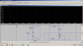
Q13, working as a diode, is not on a heatsink - it's at the top side of the board.
Q14 is actually sensing the temperature, it's placed on the main heatsink.
But which of the transistors to be mounted on heatsink where the OPS transistors are mounted? I mean thermal tracking transistors.
What is the use of the 10k NTC as i feel it can be used to sense the temperature but for what? heatsink?
I have pretty much explained it here:
NS-OPS building instructions
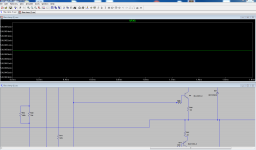
Referring to LTSpice schematic:
Q13 is not on the heatsink;
Q14, Q4, Q2 are on the heatsink;
Q17, Q18 and Q19, Q20 are on the local heatsinks (the drivers and CCSs);
NTC is not on the heatsink, sensing the ambient temperature.
I always had in thought that Jfets will have better details than tubes but I guess even tubes does it. Erno Borbley states in his article about the Telefunken tubes and jfets and he preferes jfets. I havent yet tried the tube input and would like to test the tube input version. I agree the tone of tube is always better than any solidstate but in my experience I heard alot of tubes 6sn7, 12ax7, 6GD, 300b, KT88, KT150, EL84 but they always somehow use to give over warm sound but the microdetails were not as much as jfets. Whats your call on this? I think even Jwilhelm also stated this on other thread.
- Home
- Amplifiers
- Solid State
- Ultra-high performance, yet rather simple - hybrid and more!