Lineup - There's two problems I see with your design if actually built. These are simulation vs real-life differences.
JFETs: you are running the JFETs at Idss. I've mentioned this several times. I'm guessing you only have one model for the LSJ689. You cannot buy these graded, like you can with the LSK489. Idss can range from 2.5mA to 30mA. The models available from Linear have Idss of 5.07mA, 6.84mA and 16.57mA for A, B and C grade. I attached sims at these different grades. You can see that the currents through the IPS and VAS vary widely depending on the LSJ689 grade. You can also see that the LSK489 are now running beyond their Idss range for the C grade LSJ689. This is why I suggest a pot between the sources of the JFETs and run the IPS at 2.4mA. This puts it below the lowest published Idss values you might encounter with the LSJ689. This also give you a set current for the IPS and VAS.
DC Offset: you have a pot on the emitter of the upper VAS transistor to adjust DC Offset, On your schematic this is a 200R and you have it set to 101.574 to NULL offset. However the resolution of a 25 turn 200R pot likely won't be greater than 0.5R. So it practice, you probably won't be able to adjust DC offset below 10mV or 20mV and it will vary another 50mv to 60mV from cold to hot states. If you use my suggested trimming approach, you end up with more parts but have more control over DC.
Attachments


I don't think that's a mod - its a different design. Not suggesting it's bad, just that the appeal (from my perspective) of Lineup's original design it it's simplicity.
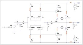
Lineup - this is my suggested changes to your design. It maintains the theme and spirit of your design, but adds in practical considerations.
- Pot P1 allows for the JFETs to run at 2.4mA. It is accommodating of any grade of LSJ689 encountered.
- The DC offset adjustment network (D1, D1, R15, R16, R17 and P3) should allow for DC to be adjusted to under 10mV. It should vary less than 20mV between hot and cold states.
- R12 & R13 allow the output bias to be measured and set.
- Reductions in R2, R5 and R6 decrease noise without otherwise affecting performance.
- R9 is increased to account for differences in capacitance between the NPN and PNP channel lateral MOSFETs
- Ground lift R14 and C8 added to ease challenges with buildings a quiet amp. A builder and put a link in for R14 and omit C8 if this doesn't appeal to them.
Attachments
What do you think about that mod?
If R21R22 and R23R24 are equal, Q11 and Q12 introduce an imbalance of currents in the input diff stage.
This gives us a distortion of about 0.0005%
This parameter in itself means nothing; you need to see with what distortions the input stage operates and the distortions at the gates of the output power transistors.
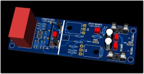
That is really beautiful 🙂And this is where I'm at with a PCB. Probably 80% there.
I prefer those JFETs in trough the hole variant. TO-71.
I see you use SOIC. That can be an idea - maybe easier to find and buy.
Nice practical modifications Brian92fs. 😉
Board layout is looking good.... faston tabs, smd JFETs👍
Board layout is looking good.... faston tabs, smd JFETs👍
I looked at both. The SOIC are 10% cheaper. Both have about the same pitch. I think the TO-71 are actually trickier than the SOIC... just my opinion.
I can likely create two different versions if there's interest.
I can likely create two different versions if there's interest.
You can use the slow boat shipping option and it's cheaper.
I use the DHL option from JLCPCB and receive my boards in 7-8 days from placing order.
I use the DHL option from JLCPCB and receive my boards in 7-8 days from placing order.
Or is that considered a stupid question?So what actually is the benefit here of using jfets in the input stage vs bjt's ?
lineup thanks for stimulating some discussion.
i am curious why no interest in the design as modified (which we have seen elsewhere: curl and hafler to name just a couple)?
no change in number of parts, just moving 2 connections that now takes advantage of the previously unused current in the other side of the diff amp.

i am curious why no interest in the design as modified (which we have seen elsewhere: curl and hafler to name just a couple)?
no change in number of parts, just moving 2 connections that now takes advantage of the previously unused current in the other side of the diff amp.
Current mirrors as a load for the diff amps should be better choice. And emitter follovers after them. Such as in #43
what will be the advantage?no change in number of parts, just moving 2 connections that now takes advantage of the previously unused current in the other side of the diff amp.
such inclusion can increase the output resistance of Q3Q4, for gate control , i think there is no “das ist gut”.
Last edited:
a simple current mirror will add modulation in temperature, in the circuit in the input Jifet above in the attachments has weak stabilization through R18.Current mirrors as a load for the diff amps should be better choice. And emitter follovers after them. Such as in #43
As an option, a Wilson mirror - but this complicates the scheme.
That should be an improvement @mlloyd1lineup thanks for stimulating some discussion.
i am curious why no interest in the design as modified (which we have seen elsewhere: curl and hafler to name just a couple)?
no change in number of parts, just moving 2 connections that now takes advantage of the previously unused current in the other side of the diff amp.
I have tested your way to DC-offset. But with a 10k pot and a 1M resistor.
I see you use 100k resistor. Would reduce input impedance, wouldn't it?
- Home
- Amplifiers
- Solid State
- Ultra Amplifier with JFET input and Lateral MOSFET out