😡The there the circuit's designer finds this one in forums electronic and down after original them de4jo the link or lace :
http://www.forosdeelectronica.com/f31/ampli-highend-clased-ucd-25w-1250wrms-solo-2-mosfets-n-24854/
http://www.forosdeelectronica.com/f31/ampli-highend-clased-ucd-25w-1250wrms-solo-2-mosfets-n-24854/
Decoupling Caps around IR2110.
Hi Baldin,
Just had a look at your schematic and breadboard amplifier. Amazing what can be done on breadboard!
In your circuit the bootstrap capacitor is larger (47uF) than the main supply decoupling capacitor (10uF). Having read through most of the International Rectifier site they recommend that the supply side capacitor C11 should be around 10 times larger than the bootstrap capacitor C14 between VB and VS which is charged through the high speed bootstrap diode.
Try swapping these two capacitors around and let us know whether it makes any difference. Might not, if a very good power supply is used as capacitors above about 4.7uF might not make a huge difference.
PeterCharles.
OK. Changed a few components, and skipped the big capacitor in the input ...
Now it starts up every time, but only with a load (speaker or 8 ohm resistor).
Switching freq is 235 kHz
Because I had to remove the big cap there is 0,6 V DC on the output .... need to find a solution ... any suggestions??
Also need ot find a way to make it start without the load ...
Otherwise it seems quite good for a breadboard circuit 😉
And I think it is an improvement over the original ........
Hi Baldin,
Just had a look at your schematic and breadboard amplifier. Amazing what can be done on breadboard!
In your circuit the bootstrap capacitor is larger (47uF) than the main supply decoupling capacitor (10uF). Having read through most of the International Rectifier site they recommend that the supply side capacitor C11 should be around 10 times larger than the bootstrap capacitor C14 between VB and VS which is charged through the high speed bootstrap diode.
Try swapping these two capacitors around and let us know whether it makes any difference. Might not, if a very good power supply is used as capacitors above about 4.7uF might not make a huge difference.
PeterCharles.
Hi PeterCharles
I have not dis-asembled the circuit yet ... so I'll try it .... if it still works 🙂
Please point to where IR writes this ..... not sure at all why this should be recommended (what significance the relative size difference should make)
BR Baldin
I have not dis-asembled the circuit yet ... so I'll try it .... if it still works 🙂
Please point to where IR writes this ..... not sure at all why this should be recommended (what significance the relative size difference should make)
BR Baldin
Hello Baldin,
1. IR Application Note AN978-b HV Floating MOS-Gate Driver ICs, page 16
2. Laszlo Balogh, Design And Application Guide For High Speed MOSFET Gate Drive Circuits, page 27
Both mentioned the size of bootstrap and bypass capacitor size.
Cheers,
WK Lai
1. IR Application Note AN978-b HV Floating MOS-Gate Driver ICs, page 16
2. Laszlo Balogh, Design And Application Guide For High Speed MOSFET Gate Drive Circuits, page 27
Both mentioned the size of bootstrap and bypass capacitor size.
Cheers,
WK Lai
Baldin,
Will see if I can find this info at some point, but will try and explain how they described the workings of the bootstrap capacitor circuit.
When the amplifier is first switched on the power supply charges capacitor at pin VCC first, then charges the Bootstrap Capacitor at pin VB through a high speed bootstrap rectifier D4. This sequence is quite important for the correct startup operation of the amplifier.
If the first capacitor is only 10uF it's charge will try to charge the 47uF Bootstrap capacitor rapidly through the diode and it would struggle to do so because the charge in the 10uF capacitor is smaller than the charge the 47uF capacitor can hold. Like trying to fill one's kettle quickly with a cup!
If the capacitor at VCC is large enough then it will hold enough charge for the Low side Driver stage and also enough charge to send to the High side driver stage and Bootstrap capacitor (through the diode) The diode prevents the bootstrap capacitor from becoming discharged by the larger capacitor at VCC when there is a large demand for charge from IR2110.
Some designers use totally independent power supplies for the High side and Low side driver stages to avoid these problems with Bootstrapping.
Hope it makes sense that the bootstrap capacitor should be smaller (easier to keep it topped up from the bigger capacitor) 😀
PeterCharles
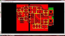
So this saga continues, heres the daughter board with the MAX913 on it:

Yeah i know the layout isent that great but it was my first ever smd job and after all none of the long traces carry more than audio signals so it should be ok, atleast for a prototype.
Yeah i know the layout isent that great but it was my first ever smd job and after all none of the long traces carry more than audio signals so it should be ok, atleast for a prototype.
hope they come fast.... i am very curious ...
attached is almost complete pcb design made with only smd parts.
regards,
savu
Very compact PCB design! Very curious to know its performance.
Cheers
hope they come fast.... i am very curious ...
attached is almost complete pcb design made with only smd parts.
regards,
savu
can you post the files (also for the schematic with values - that way it can't be mixed with other versions of this amplifier)?
I was thinking about etching one of these. I have a bunch of PCB material I've had around for a while and want to do something with them.
I'm guessing it can't do 1200 watts with just 2 output devices? What kind of power do you guys expect/get with this smaller board?
The SMT board looks very nice indeed 🙂 I just need to pick a design and get to etching it lol.
I'm guessing it can't do 1200 watts with just 2 output devices? What kind of power do you guys expect/get with this smaller board?
The SMT board looks very nice indeed 🙂 I just need to pick a design and get to etching it lol.
Hello Gents,
as i speciffied the pcb is partialy finished. it misses the supply filter caps, the imput resistors and caps, the feedback loop, and the output LC filter.
when it's done i will post complete pcb design with part values.
regards,
savu
as i speciffied the pcb is partialy finished. it misses the supply filter caps, the imput resistors and caps, the feedback loop, and the output LC filter.
when it's done i will post complete pcb design with part values.
regards,
savu
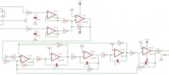
A bit faster level shifter
Hello Tekko,
If you add a 10pF cap parallel to R3 or R15, you will get a bit faster level shift.
Cheers,
Here is the sim,
Heres a simulation of what im gonna try when the MAX913's arrives.

Hello Tekko,
If you add a 10pF cap parallel to R3 or R15, you will get a bit faster level shift.
Cheers,
Here is the sim,
An externally hosted image should be here but it was not working when we last tested it.
Last edited:
Hello Gents,
as i speciffied the pcb is partialy finished. it misses the supply filter caps, the imput resistors and caps, the feedback loop, and the output LC filter.
when it's done i will post complete pcb design with part values.
regards,
savu
I think I may try your board once it's finished.
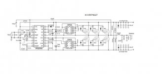
I've got a problem with Ejtagle UCD when driving 12 inch woofer..
I've got a chance to drive 12 inch JBL speaker GT01214 with my UCD.. I used the following lowpass filter but the amp could not drive the speaker after a certain level that It produces clipping noise for drum foot.. I wish thats before clipping level. but when I use this filter with a class AB amp (DX standard by Carlos), the woofer drives well without any clipping noise.. also can volume more than my UCD to drive the woofer well enough and have a good output power (good bass). My questions is that its because of class AB clipping noise is not audible ?? or if not whats wrong with my UCD over others ?? I dont have a scope to measure but theres a huge difference between those 2 amps.. used the same supply for both +/- 50v. that is true I increase the gain of the low pass filter to fit my input source... and I can assure that its not the issue because of both the amps give almost equal output at same level of input.. some professional advice is needed.
Thanks in advance and best regards,
Lycanlk
Attachments
Hello Tekko,
If you add a 10pF cap parallel to R3 or R15, you will get a bit faster level shift.
Cheers,
Here is the sim,
An externally hosted image should be here but it was not working when we last tested it.
And two more capacitors are added directly from comparator outputs to HIN and LIN gate driver inputs, it's even faster. The optimum capacitance value may be lower than 10pf. But this requires clean supply rails, any substantial Mhz ripple on the negative rail WRT ground will make it unreliable, and your PCB layouts are likely to produce plenty of that.
Last edited:
- Home
- Amplifiers
- Class D
- UCD 25 watts to 1200 watts using 2 mosfets