OK, one PCB per mono amp, that's clear.
Less PCB-s, less wires, less interferences, the better. 😎
Yep are are we buiding....HP or not HP...then the better we can..the better it must be😎😎😎
Marc
It is missing Gerhards, input pair and the trimmers which will be added.
But until now i would like to get the SCH confirmed.
Your schematics is just fine according to post #330.
As we lately also spoken about Sziklai/Baxandall input pairs and output improvement, please look to my latest post TSSA Basic 1.4 where all these new features are already included. 😉
I think we have to have each part of three main stages put to high performance and 1.4 version follows that. 😎
Sonny... are you sure that the bias-spreader works when you take the signal out on the drains..??
Yes, why dont you Think so? MiiB ?
I also havent added the jfet to the bias and dc settling circuit. This Will be done.
Andrej, you added a source follower to the output mosfets. That was exactly was i meant!
I also havent added the jfet to the bias and dc settling circuit. This Will be done.
Andrej, you added a source follower to the output mosfets. That was exactly was i meant!
TSSA Basic 1.4 - Sziklai input, buffered output
Telepathy present again in this thread.
Yes, we spoke about isolating input stage from the output's stage load current. This additional MOSFET driver would do just that. OK! 😎
In attachment is TSSA Basic 1.4 with Sziklai inputs. Sonnya I think the Sziklai input pairs would be manageable, much more than Baxandall ones, since the input bias current is much more defined Ic=Vbe/Rbe=0,65 V/1 kohm=0,65 mA. Which of them to include in your schematic and consequently PCB? 🙄
Regards, Andrej 😉
Andrej, you added a source follower to the output mosfets. That was exactly was i meant!
Telepathy present again in this thread.
Yes, we spoke about isolating input stage from the output's stage load current. This additional MOSFET driver would do just that. OK! 😎
In attachment is TSSA Basic 1.4 with Sziklai inputs. Sonnya I think the Sziklai input pairs would be manageable, much more than Baxandall ones, since the input bias current is much more defined Ic=Vbe/Rbe=0,65 V/1 kohm=0,65 mA. Which of them to include in your schematic and consequently PCB? 🙄
Regards, Andrej 😉
Attachments

Last edited:
because the bias is set via the voltage diffidence from Rail to gate and not like conventional a voltage between the two gates
Sonny... are you sure that the bias-spreader works when you take the signal out on the drains..??
I now Think i know what you mean!
The buffer has its drains connected. They need to be separated through a GND or connected to the output.
because the bias is set via the voltage diffidence from Rail to gate and not like conventional a voltage between the two gates
It is fully ok to do it this way. The mosfets are now comparable to a VAS, you just have a higher idle current like in the MF A1 or the "le monstre 8w" (even in the early nineties it was difficult to get the bjt!)
It is fully ok to do it this way. The mosfets are now comparable to a VAS, you just have a higher idle current like in the MF A1 or the "le monstre 8w" (even in the early nineties it was difficult to get the bjt!)
The source is connected to the rail
If you want to equalize Ugs of the J-Fets a resistor could be inserted between source and collector.
Last edited:
Yes Gerhard, in that way we would have exactly the same power dissipation on pos/neg input compounds. That also means two more resistors to calibrate by measuring and matching both Ugs. 🙄
I think it is easier to glue all four input BC-s to the small metal plate, two faces from one side (inputs) and another two faces (Sziklais) from another. In that way all four would share the same temperature, which would stabilize bias and DC offset conditions to perfectly normal level.
I think it is easier to glue all four input BC-s to the small metal plate, two faces from one side (inputs) and another two faces (Sziklais) from another. In that way all four would share the same temperature, which would stabilize bias and DC offset conditions to perfectly normal level.
TSSA Basic 1.4 - Sziklai input, buffered output
Buffer's drains connected to GND.
The buffer has its drains connected. They need to be separated through a GND or connected to the output.
Buffer's drains connected to GND.
Attachments

366 goes in the right direction i think.
Yes agree completely, hehehe I will stop for a while with #374, now it's Sonya's move. 😀
I even have all the parts. Could build it p-p tonight
Be my guest. I would not build the 1.4 as p-p. 😀
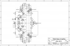
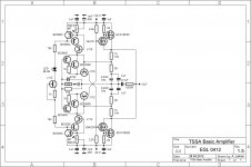
Check this one.
The input pair will be placed very close. And everything will be placed in groups.
Attachments
TSSA Basic - Sophisticated Stages
Very good Sonnya, your schematic is OK, only the output stage still to correct.
Look in the mean time (few seconds hehe) I was thinking that buffer stage is one more stage which is not present in post #1, so that would be out of the concept of three stages only. 😎
So I decided that output device must be compound one in a same way as the others are. Output Darlington MOSFET is just the right solution, driver's drain connected to the output. 😉
Voilà, here we have it, TSSA Basic schematic to go for.
Be my guest. I would not build the 1.4 as p-p. 😀
Check this one.
The input pair will be placed very close. And everything will be placed in groups.
Very good Sonnya, your schematic is OK, only the output stage still to correct.
Look in the mean time (few seconds hehe) I was thinking that buffer stage is one more stage which is not present in post #1, so that would be out of the concept of three stages only. 😎
So I decided that output device must be compound one in a same way as the others are. Output Darlington MOSFET is just the right solution, driver's drain connected to the output. 😉
Voilà, here we have it, TSSA Basic schematic to go for.
Attachments
- Home
- Amplifiers
- Solid State
- TSSA - The Simplest Symmetrical Amplifier