I followed the circuit diagram to a T and all i got was noise when i plugged it all in. i am running a balanced 1/4" output into the circuit and going directly into the amplifier board signal input with it.
what am i doing wrong?
what am i doing wrong?
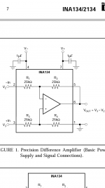
I used the exact schematic on the Texas instruments technical document for line receiver. I used a 13.5 volt DC regulated power supply on the v+(pin 7)/v-(pin 4), they each have a 1uf cap going to ground...trs ring going into pin 2, tip into pin 3, tied pins 5+6, tied pin 1 to ground. Then used pin6 as the + output and pin1 as the sg into the amp board. I wasn't 100% sure where the shield should connect from the trs input. Need help with that one. Anyhow, I got nothing but noise out of the chip.
Attachments

Does anyone know of a proper circuit board kit to do something like this for sale anywhere? This was just a test circuit to see if I could achieve cmr on my amp inputs. My final build ideally should have better than a breadboard.
As stated before: show your schematic and:
describe the noise (hum, crackling, hiss, sounds not suitable for refined company, etc.) E
describe the noise (hum, crackling, hiss, sounds not suitable for refined company, etc.) E
The noise is just that, it has all those characteristics. Hum, hiss...etc I originally just ran the amp unbalanced from my audio interface line output (focusrite ls56) but it proved to have noise over the fire wire cable. Digital noise from the computer. It was silent when using an ipod unbalanced. My other powered studio monitors have balanced inputs and there is no noise on those so I want to add balancing to the new amplifier inputs as I will be driving new higher end passive monitors in the studio.
quote....... I used a 13.5 volt DC regulated power supply on the v+(pin 7)/v-(pin 4), they each have a 1uf cap going to ground..........
do you use a single supply? the ina - schematic is for dual supply.......
do you use a single supply? the ina - schematic is for dual supply.......
Took a look at an003 it just shows how to do the same thing using a transformer instead of an active Chip to receive the balanced signal. This ina134 Chip should have no issue doing it for a much cheaper cost.
quote....... I used a 13.5 volt DC regulated power supply on the v+(pin 7)/v-(pin 4), they each have a 1uf cap going to ground..........
do you use a single supply? the ina - schematic is for dual supply.......
It only uses one power input to run the chip. The other inputs are the hi and lo signal inputs from the balanced output.
If you want useful advice you really have to give more details. Draw a complete schematic. Measure DC at ALL the pins of the INA. The whole power supply setup is very unclear - draw a schematic!
Where do the signals come from? Are the two signals on the inputs the same or are they in opposite phase? How is the connection to the chipamp done, what is the schematic of the chipamp? Does the chipamp work on itself, and how do you know?
Tell us the details!
Jan
Where do the signals come from? Are the two signals on the inputs the same or are they in opposite phase? How is the connection to the chipamp done, what is the schematic of the chipamp? Does the chipamp work on itself, and how do you know?
Tell us the details!
Jan
Problem solved. and i think this might be the first public link to the proper solution for a beginner without in-depth knowledge of circuit design.
Balanced Input Building Block – DIYRE
This kit solves the balanced input creation for any amplifier unbalanced input.
enjoy!
Balanced Input Building Block – DIYRE
This kit solves the balanced input creation for any amplifier unbalanced input.
enjoy!
Well the problem isn't solved until it works! 😉
It's a pity you didn't chose the path to understanding it yourself....
Good luck!
Jan
It's a pity you didn't chose the path to understanding it yourself....
Good luck!
Jan
Honestly, I wish I could, I built the circuit the way it showed on the schematic exactly, I even had my father who is an electronic engineer look at it, and it seems right, this board kit I found uses the same Chip, but does more with caps and stuff. It's like French to me. I don't plan on going to school to understand why this resistor or that works the way it does and this or that value of capacitor. I want the thing to work when I make it the way it shows. That's it. I anyone wants to elaborate on how this Chip schematic I posted actually operates and why it does what it does, i'm all ears but I won't go out of my way to figure it out myself!
You missed a lot of opportunities here.
Nobody wants you to figure it out on yourself, but if you're not even up to the task to tell us in detail what you've done, hey, why do you think it will be different with that ready-made board??
Beats me.
Jan
Nobody wants you to figure it out on yourself, but if you're not even up to the task to tell us in detail what you've done, hey, why do you think it will be different with that ready-made board??
Beats me.
Jan
Did I miss something on the explanation of what I did? I have a balanced output coming from an audio interface, of which I do not have a schematic for it, but I do know that it creates a typical balanced signal on trs with tip hot, ring cold, and sleeve ground. The hot and cold signal are out of phase as per any balanced output, then this ina 134 circuit (schematic posted) is supposed to accept the hot and cold signals, flip the phase of one, combine it with the other and noise will then be out of phase across the two and cancel out. Does not matter the details of the amplifier the signal is going into. The amp works fine on its own. It's the signal I'm trying to change.
There is digital noise on the ground coming into the interface from firewire and this circuit should in theory get rid of it just like the input on my powered monitors do.
It only uses one power input to run the chip. The other inputs are the hi and lo signal inputs from the balanced output.
Your answer to this question still concerns me. The INA134 is designed to run from DUAL power supplies, which would mean you should have +13.5V on the V+ pin and -13.5V on the V- pin. Or if running from a single supply you should bias the REF pin up to the mid supply point (13.5V/2) from a low impedance source (not a voltage divider) and AC couple the inputs.
An output from a DC power supply has a + and a - wire coming out of it. One is + 13.5 vdc, the other is - 13.5vdc. How would you need more power than that? Use 2 separate power supply units, run + of one to the v+ with - to ground, then the second unit run - to v- and + to ground? I'm doubly confused now!
- Status
- Not open for further replies.
- Home
- Source & Line
- Analog Line Level
- Trying to make a Balanced line input on LM3886 chipamp using ina134. HELPPP!!!