I'm having this issue in my design where I have to warm up Q1 and Q7 with a finger to get idle current flowing. Once it's going, I can adjust the current and it stays fairly stable.
One stage at a time...
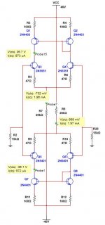
Is there any reason these DC operating points wouldn't be sufficient to drive the VAS? 36.7V at the mirror/LTP collectors is 2.7V more then the VAS Vbe of ~0.6V.
One stage at a time...
Is there any reason these DC operating points wouldn't be sufficient to drive the VAS? 36.7V at the mirror/LTP collectors is 2.7V more then the VAS Vbe of ~0.6V.
Attachments
That should not be happening. You sure it's not oscillating? Or you forgot a connection? How do you adjust?I'm having this issue in my design where I have to warm up Q1 and Q7 with a finger to get idle current flowing
I took the liberty of plonking it in LTSpice and the results are identical. See the attached ZIP file.

Attachments
Last edited:
It's really not that complicated of a circuit. DC offset is a good indicator of fault but that's been great at about ~2mV. The new PCBs make probing around quite difficult. I intend to make another set of test PCBs that allow me easier access to connect leads and make measurements. I guess I'll transfer everything from the non-working unit to the test boards and try to find what's wrong.
Output stage idle current is adjusted with a trim pot between base to emitter on the VBE multiplier. That transistor is clamped to the heatsink between the output transistors. Once everything warms up I can adjust the idle current to say 20-40mA and for the most part it'll stay there. It's at cold start-up that there's no idle current. As if I'm near the Vbe threshold of a device. The VAS even has 100R emitter degeneration (bypassed with 0.1u cap) to improve bias stability.
In the circuit above, how tolerant is it to temperature? Can you throw off the Vbe a bit in simulation and see if it gets badly imbalanced?
Last edited:
You make PCBs? I'd just use prototyping boards. So much easier. Once the whole shebang works only then I make PCBs.
You cannot do useful offset/temperature tests with only the input stage.
You cannot do useful offset/temperature tests with only the input stage.
I was curious if a variation in Vbe may cause the CM or LTP to drop out. Thus sending the CM to LTP collector junction too high to draw current from the VAS base. My thought is that nothing downstream of the IPS matters if the VAS drops out and/or the output stage isn't conducting.
The current circuit was first built on breadboard. It worked fine. Then I ordered PCBs (3x for $80) to make a home amp version. They work fine. Then I transferred to smaller PCBs that are intended for small monoblock amps for my car. That's when the error happened. I've gone over the layout at least a dozen times and can't locate any errors. The amp does play. Sounds good. It just powers up in class B. If I let it play awhile and warm up on it's own it'll eventually get back into AB. Being a mobile application, it will see winter and summer use.
So long story short... I figured I'd post it here and go through each stage step by step and verify that I either made an error or I'm going nuts. The output from the IPS circuit above shouldn't have any issue driving the VAS. Seems you concur?
Last edited:
You need to post the whole schem.
Are you using different parts and transistors in this smaller version than the ones that work as expected? Or is it only the PCB and layout that is different?
Are you using different parts and transistors in this smaller version than the ones that work as expected? Or is it only the PCB and layout that is different?
Yes, please post the whole schematic. The whole raison d'être of the input stage is to inject base current into the VAS transistor(s). Looks like it can do that. It operates in class A, anything else is unacceptable because it will not be able to control the output. VAS is class A as well, same reason. Only the current stage (output) can completely switch off its current. If the polarity of the signal allows this of course.
If you have versions that work you must have introduced an error somewhere. Scope/multimeter will reveal where.
If you have versions that work you must have introduced an error somewhere. Scope/multimeter will reveal where.
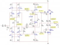
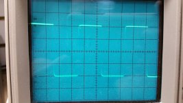
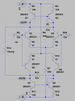
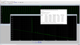
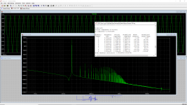
This is what the problematic PCB is based on. The CM in this uses 5401/5551 vs the 4401/4403 in the previous schematic I posted. Also attached is a 20kHz squarewave this circuit produced from the two working PCBs. The zener in the Vbe multiplier divider helped stabilize the bias when the supply rails are lower.
Attachments
Try and calculate the vas current yourself - no simulator! This problem has been discussed in many threads on diy audio.
To explain it a bit better, get your simulator to start the supplies at 0V DC and ramp them up. You will see that the initial DC conditions in the VAS are not defined, and this prevents the amplifier starting up.
By warming up Q1/Q7, you are creating an imbalance which causes a DC offset. This offset gets things going. Adding cascodes will also create a stable DC point which will do the same thing.
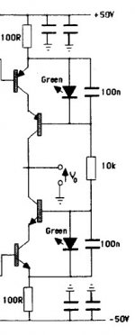
If you're going to do anything, i'd suggest cascoding the VAS - use the BD139/140 as the cascodes and use small signal transistors as the actual VAS transistors. Like so.
By warming up Q1/Q7, you are creating an imbalance which causes a DC offset. This offset gets things going. Adding cascodes will also create a stable DC point which will do the same thing.
If you're going to do anything, i'd suggest cascoding the VAS - use the BD139/140 as the cascodes and use small signal transistors as the actual VAS transistors. Like so.
Attachments
Any other tricks? I don't have the room for 7 more components unless I add a another daughterboard.
That's another option. I can't visualize how the mirror causes a problem but I have read they can be troublesome.
Symmetry topology with current mirror is first introduce by Randy Sloane in his book. But it worked intermittent because, current of VAS's colector did not determine. Bob Cordell in his book add solution with resistor in colector of current mirror, so the DC voltage of all transistor in the current mirror always same. The current of VAS's colector now determined. Then Dr. Arto Kolinnumi add constant current source as base current of VAS transistor. Because base current is small, the constant current source can be replace by high value resistor (R14).
Attachments
Current mirrors on a symmetric LTP input is a bad idea because the two diff amps do not agree on the DC offset. The result is that the two VAS transistors fight each other in an effort to get their way, iether with too much or too little VAS current, hence too much or too little idle bias. If you must use a symmetric IPS, you have to load them with resistors and not current mirrors.
Edmond Stuart made solution with common mode current loop (CMCL), but it more complex. You can find it in this forum.
Current mirrors on a symmetric LTP input is a bad idea because the two diff amps do not agree on the DC offset. The result is that the two VAS transistors fight each other in an effort to get their way, iether with too much or too little VAS current, hence too much or too little idle bias. If you must use a symmetric IPS, you have to load them with resistors and not current mirrors.
If I chose to load using resistor, which VAS topology works best, darlington or CFP, when driving mosfets? THD (in sim) is going to go through the roof with just a resistor load.
Last edited:
- Home
- Amplifiers
- Solid State
- Trouble with HEXFETS