Hello guys.
To be honest, I become desperate.
I have already made one good headphone amp with 1 TPA and differential OP1642 (not I/V), PSU was +-6.5V. It has a very clean output, without noise.
Now I'm working on a fully balanced headphone amp with opa1642 as an I/V and then again the same OP as a non-inverting amplifier. I'm driving the headphones with TPA6120A2 as a buffer, 1k is in the feedback, voltage is +-15V.
When I've tested it I heard little noise with the IEM of 32ohm, and much more noise with IEMs 16 Ohm, not sure about sensitivity but pretty sensitive.
SNR of this AMP is 10db worse than the first amplifier.
In the end, I made another 2layer PCB just with OPs, without any switching ICs. I've also tried the first PSU +-6.5V which was good for the first AMP, I really don't think it is up to the PSU (Tried to filtered even more but there wasn't any result). I desolder OP1642 and leave just TPA and his non-inverting inputs connected to the ground through a 4.7k pulldown resistor, but then I also had noise, the same level or similar.
DC offset is good, about 2mV. When I connect inputs of TPA to the ground then I have dead quiet outputs, but when I connect it on some resistor or OP I have some noise. Is It normal? Why the first amp is so better. Can I do something?
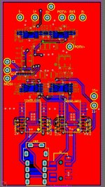
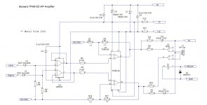
Can you post a circuit and a picture of your PCB layout- very difficult to help without this basic info.
Can you post a picture of your layout?
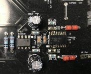
Here is a picture of mine. My gain is set to 6x and it works superbly.
Here is a picture of mine. My gain is set to 6x and it works superbly.
Attachments
Last edited:
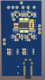
Pictures are attached.
If you didn't try it with sensitive iEM or measured SNR you can't know is it really clean. I can hear very little noise with the standard 32-ohm iEM that comes with the mobile phone, and much more with a good 16 Ohm iEM.
If you didn't try it with sensitive iEM or measured SNR you can't know is it really clean. I can hear very little noise with the standard 32-ohm iEM that comes with the mobile phone, and much more with a good 16 Ohm iEM.
Attachments

Last edited:
These schematics are confusing as hell. Did a circuit of this relatively modest complexity really have to spread out across 4 entire pages, out of order no less? And who in their right mind orders their input pins L- / L+ / R+ / POTV / 3V3 / R-? First rule of differential signalling, always treat your signal pair as one and keep + and - closely together.
You are using the TPA6120A2 is a noninverting unity gain configuration, why? This is not how these are normally used (see datasheet) - they presumably are not optimized for high common-mode input voltage swing and can be hard enough to keep stable in the regular inverting unity gain configuration with its lower bandwidth. (There is a reason why the datasheet suggests 10 ohm series resistors, although apparently lower output impedance is very much achievable.) This is just begging for trouble, especially when you could go inverting and switch your input signals around accordingly. (Don't forget adding the resistors!) Oscillation can manifest as excessive noise.
Also, here's the obligatory reminder that this chip generally isn't very fond of driving low-impedance loads <64 ohms. Good heat transfer via the exposed pad at the bottom of the chip to a decent amount of copper on the board is the minimum I would suggest.
I hope you have read up on the caveats of using just one half of an ESS DAC output, as you are doing when the SE output jack is being used.
I am not sure I would recommend following up the NJW1195A output with a gain of +8.1 = +18 dB either. That's a guaranteed 1.26 µV x 8.1 = 10.2 µV of output noise right there (-99.8 dBV / -97.6 dBu), 3 dB more in balanced mode. Given that the chip can output plenty by itself, I wouldn't think more than 6 dB of gain is necessary here. If driving sensitive loads is a priority, I would think about a unity gain option as well.
Last edited:
Thanks, I believe that it is up to the non-perfect single-end signal from the DAC that is expected to be used as a Differential. When I use differential OP-AMP topology I don't have that problem because in that case OP cleans every common mode noise from the + and - signal. When using just + signal I don't have that advantage. I will try to use fully differential OP, if I have understood it well, it will clean that noise and give me + and - signal as I want, not a single end.
Pay careful attention to the Zobel network and the 3.3 Ohm resistors in series with the output.
In addition, the TPA6120 is a CFA device - so very wide BW. Layout is critical - you don’t want any excess capacitance from the inverting input to ground (or any other supply pin) as this will create an additional zero in the response and lead to instability. So, make sure the ground plane is cleared from around the - input.
In addition, the TPA6120 is a CFA device - so very wide BW. Layout is critical - you don’t want any excess capacitance from the inverting input to ground (or any other supply pin) as this will create an additional zero in the response and lead to instability. So, make sure the ground plane is cleared from around the - input.
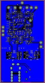
I also made a 4-layer PCB, so my idea is to maybe clear all 4 layers under TPA. I had no problems with the last layout, there was a small TPA package.
At this 2-layer test board, I cleared planes under TPA and I still have noise. The conclusion was that it was from a noisy input, don't know where that noise coming from, even when I put 4.7k ohm (or smaller) to the ground on the input, without anything else.
I tried with the series resistance at the output, maybe also the Zobel network but I'm not sure.
It’s specifically the parasitic capacitance from the inverting input to 0V or the + or - rails.
The TPA6120 must be fed from a low Z source.
The TPA6120 must be fed from a low Z source.
- Home
- Amplifiers
- Headphone Systems
- TPA6120A2 problem with noise