Hi.
Couldn't get answers in another dead thread, so here goes:
Got these boards from China and am delighted with them EXCEPT the gain is way too high for my application (triamplified speakers in a conventional hifi system).
Gain seems to be ~32-35dB, and my other amps ~27dB.
I have read that the boards use two resistors in a voltage divider to set the gain.
Attachments
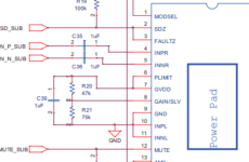
The pinout diagram for y TPA3118 shows a 47k and 75k resistor in the gain-setting voltage divider.
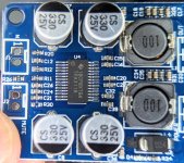
I see R11 & R12 and think these may be the ones to change(I even read removing the larger value will give a gain of 20dB). I'm not experienced nor confident enough to make changes without some positive confirmation. Anyone here have experience changing/removing the tiny SMD resistors and which one to remove? Thanks
I see R11 & R12 and think these may be the ones to change(I even read removing the larger value will give a gain of 20dB). I'm not experienced nor confident enough to make changes without some positive confirmation. Anyone here have experience changing/removing the tiny SMD resistors and which one to remove? Thanks
Attachments
Reading the device Datasheet
I use two hot soldering irons to remove passive smt. After I use some solder wick to clean the pads so the replacement device sits flat. A small bit of solder on one pad, tweezers to place, center new device, reflow and then add a bit more solder onto pads to finish off. Hint do not let hot iron tip touch the end terminations.
I use two hot soldering irons to remove passive smt. After I use some solder wick to clean the pads so the replacement device sits flat. A small bit of solder on one pad, tweezers to place, center new device, reflow and then add a bit more solder onto pads to finish off. Hint do not let hot iron tip touch the end terminations.

R12 on your board is 47K (473 on the resistor means 47 X 10 to the third power = 47 K). R11 is 75K (753 on the resistor). You can see in your board picture that pin 6 goes to R12 and pin 9 goes to C26 and R11. That matches the schematic you posted. From the datasheet, are the different gains you can choose:
R12 R11 Gain, dB
47K 75K 36
39K 100K 32
20K 100K 26
5.6K Open 20
R12 R11 Gain, dB
47K 75K 36
39K 100K 32
20K 100K 26
5.6K Open 20
Brilliant! Thanks 🙏
One more question:
What gain results if R12 remains at 47k and R11 is open? (The easiest for me, since the components are so tiny and I have no SMD soldering skills)
Thanks and best wishes
-Chuck
One more question:
What gain results if R12 remains at 47k and R11 is open? (The easiest for me, since the components are so tiny and I have no SMD soldering skills)
Thanks and best wishes
-Chuck
You should get 20 dB gain. Read section 7.3.1 of the datasheet for a full explanation. Do note that at 20 dB gain (10X voltage gain) you'll need an input voltage of 1.41 Vrms to get full output (50W into 4 ohms). The good news is the 20 dB gain setting has the the best SNR (less potential hiss).
Please, can you provide a link to this Datasheet? I can't find any references to gain settings where I looked. Thanks & best wishes -Chuck...From the datasheet, are the different gains you can choose:...
- Home
- Amplifiers
- Class D
- TPA3118 PBTL Gain issues