Used them lots of times, they're great, never had a bad PCB.
I use them, dirtypcbs.com, elecrow.com and iteadstudio.com - I'm pretty certain all of these companies order from the same board house though, as the quality, manufacturing specifications, color options, etc... is consistent across all of them.
Thanks gmarsh. They offer incredibly low prices, and just waiting to hear if the shipping cost to UK makes them more economical choice. I'll give the others you mention a browse too.
Best UK price is £20 per board all in. Seedstudio are £2 per board before shipping!
Found 3116 on aliexpress at £8 for 5 IC's delivered to UK if I solder myself. Starting to see how China knocking out the amp boards so cheap now....😱
Saturation by itself doesn't cause inductors to heat up, most heat will come from the DC resistance of the inductor windings and the RMS current going through them. If you're amplifying music, the RMS current is fairly low.
Even with 2A RMS (say) and 20mohm inductors, that's 80mW copper loss. In a 12mm inductor package that's barely noticeable. There will be some hysteresis loss too, but it'll probably be a small fraction of that.
Even with 2A RMS (say) and 20mohm inductors, that's 80mW copper loss. In a 12mm inductor package that's barely noticeable. There will be some hysteresis loss too, but it'll probably be a small fraction of that.
Referring to CuriousOne problem.... Could it be DC Detect doing this if input caps are rubbish? I know I had awful problems with the stock input caps at start!
Looking for clarification I understand the circuit connecting SDZ to GND through switch, for standby.
I need to separate the "normal" SDZ / Fault pin connection and give each their own 100k resistor to PVCC.
I then fit a switch between PVCC and SDZ which goes to ground. I presume on the SDZ pin side of the resistor.
Does this standby switch circuit work alongside the gvdd / mute mod OK?
I am thinking slotting in a LED+resistor in the SDZ switch to ground line to light up when put in standby mode.
Anyone got experience of Seeedstudio pcb's and service?
I have used them twice...no errors on any boards.
Boards also looked good.
I have used them twice...no errors on any boards.
Boards also looked good.
Thank you DUG. Other reviews I have seen support this view also.
they got back to me with shipping estimate to UK as around $30. That means I can get 5 bare pcb's from them for $49 all in. Whereas made in UK cheapest found works out $31 for a single pcb. I can get 5 tpa3116d2 from ali-express for $12, so as long as I solder myself I get component ready board for just over $12. Less than 50% of UK boards. Stupid rulers of our nation pricing us out of global economy!!!

Looking for clarification I understand the circuit connecting SDZ to GND through switch, for standby.
I need to separate the "normal" SDZ / Fault pin connection and give each their own 100k resistor to PVCC.
I then fit a switch between PVCC and SDZ which goes to ground. I presume on the SDZ pin side of the resistor.
Does this standby switch circuit work alongside the gvdd / mute mod OK?
I am thinking slotting in a LED+resistor in the SDZ switch to ground line to light up when put in standby mode.
You leave SDZ/FAULTZ connected and wire:
PVCC -> LED_anode -> LED-cathode -> R_10k_in -> R_10k_out -> SDZ/FAULTZ -> R_100_in -> Shutdownpin
You will then pull this pin low to enter shutdown. (This will also lid your LED)
PVCC ^-- ->|- -[10k]- -(SDZ/FAULTZ)- -[100R]- --°Pin
PVCC -> LED_anode -> LED-cathode -> R_10k_in -> R_10k_out -> SDZ/FAULTZ -> R_100_in -> Shutdownpin
You will then pull this pin low to enter shutdown. (This will also lid your LED)
PVCC ^-- ->|- -[10k]- -(SDZ/FAULTZ)- -[100R]- --°Pin
Maybe it's just the luck of the draw. These Chinese amps are very inconsistent in build quality even from the more reputable sources.
You leave SDZ/FAULTZ connected and wire:
PVCC -> LED_anode -> LED-cathode -> R_10k_in -> R_10k_out -> SDZ/FAULTZ -> R_100_in -> Shutdownpin
You will then pull this pin low to enter shutdown. (This will also lid your LED)
PVCC ^-- ->|- -[10k]- -(SDZ/FAULTZ)- -[100R]- --°Pin
Thanks. I think I get that!
Do you mean the R_10k's before & after the LED? And with the LED they are where the R_100k is in stock circuit, with a new 2nd trace from SDZ/faultz to shutdown switch via R_100, then to GND?
leaving aside my mistake of disconnecting SDZ/faultz, as the HSDZ boards I got at moment have a "R_10k-> led->GND" off of the VCC input for a power on light, I thought my suggestion of having the R & LED between pin and gnd would have worked. Will it still work if I left the
PVCC->R_100K->SDZ/FAULTZ as is, then add the
SDZ/FAULTZ->100R->PIN->R_10K->LED->GND
The reason I would prefer layout as I suggest is that I would want the "standby led" as well as pin/switch off board on enclosure front panel, and would prefer not to take the pvcc trace off-board and then back to SDZ/faultz, if my suggestion above works it means I could wire straight to central 3116 GND point as well. I could then just have the 100R/pin trace and a ground via on the PCB if led not wanted.
Last edited:
Should do, like so:
http://www.ldcooling.com/shop/70-57...itch-19mm-black-housing-ring-illumination.jpg
?
http://www.ldcooling.com/shop/70-57...itch-19mm-black-housing-ring-illumination.jpg
?
Aye. That sort of thing. Can get many different designs. Seen some with pc/Xbox symbol light, some in chrome, some in stainless, some gold etc....
Think depending on how you wire, it can be light on when off, or when on. I'll fit in circuit and try and test out on spare board.
I have used them twice...no errors on any boards.
Boards also looked good.
Could I ask DUG, and same question also applies to gmarsh weiner board,
How do you find comparison VCC traces around outside of board against up through the centre then transferring layers to go to either side?
I can see the positives, and negatives in both implementations against the "theory", but left wondering if it's a big issue on this size of board, or just a question of layout preference!
Not wishing to cause offense, or argue with either party, or cause arguement between designers. Would just like opinion of both implementations...

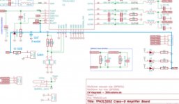
I like using fat polygons for power and anything else that carries high current, excepting fast dv/dt stuff like the OUTxx pins on the TPA. I also try to keep the underlying ground plane as unbroken as possible.
My card and DUGs card are laid out largely the same this way, with the left/right hand sides of the TPA chip being fed separately. I feed my power planes underneath the inductors (I can with my TH inductors) while DUG feeds them around the board perimeter.
My card and DUGs card are laid out largely the same this way, with the left/right hand sides of the TPA chip being fed separately. I feed my power planes underneath the inductors (I can with my TH inductors) while DUG feeds them around the board perimeter.
I would have liked to have a more direct route (pardon the pun) for power but that was not feasible for the size and variety of inductors I designed for. I could have rotated the inductors to allow the supply to go beneath but that would have increased the board size or made the inductor soldering difficult.
Design is about choices and compromises.
Design is about choices and compromises.
Thanks chaps. I thought that component choice would play a strong role, and of course compromise.
Just asking as wasn't sure if preference, or performance was a factor. Theory tells me outside of pcb is "a no-no" for power traces, but same goes for the up through centre weaving around other "signal" traces and components. But as your boards demonstrate both options, the performance of either isn't factor.
The HSDZ "YJ blue/black copies" have an interesting way of traces from input under the board to one DC power cap, with a trace breaking off and going straight across to the other power cap positive. The one going across board roughly goes across under the IC output side pins. I suppose it kind of combination of different factors. Under board surrounds VCC with GND, keeps it away from input or output traces on top. the trace between caps does semi-cut the GND plane in two, but in a good way between input & output side. With its power GND traces IC GND to DC power caps on top layer, away from GND plane.
I'm only designing board for my use, so my layout/implementation will dominate. As I am planning for pcb set in larger "boxed" enclosure with linear power supply and pllxo I am playing around with vcc/GND & output connection locations to see how it affects layout, and location in enclosure, which will be more more rounded curved than box, bit like a "MINSTRAL" chocolate sweet shape - sort of flying saucer shape, using wood ply.
Thanks again for views regarding the power traces on your boards.
Realised last night, very late, that I forgot to say thank you to Doctormord for his input with my SDZ/FAULTZ standby question. So many thanks Doctormord. I am just left with choosing just one design of latching switch from the hundreds available 😕
Last edited:
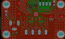
For your PCB inspiration,.

Interesting. Don't know the chip too well, but those VCC traces look similar implementation to HSDZ.
Can I ask why the lack of vias in the "U" shape down from VCC points around output section?

Oh.... Is that the VCC trace underneath? Oops.
- Home
- Amplifiers
- Class D
- TPA3116D2 Amp