I can tell from own experience that K3497/J618 has huge positive tempco.
Much worse than IRFP240, 2SK1530 etc.
If you watch carefully, he bolted the TO220's directly on top of the TO247s for thermal coupling.
No heatsink in between.
I guess that in this particular configuration, the positive tempco of the TO220s more than compensates that pf the TO247s.
The devices are all obsolete.
But maybe the idea can still be used for IRFs or Fairchilods ?
One can only find outexperimentally though.
Kamijo san has many interesting ideas that I keep going back to.
He passed away in 2012, sadly.
Someone is keeping his website alive, but may not be forever.
Patrick
Hi Patrick,
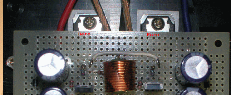
The TO-220's are the bias generator MOSFETs.
That makes sense now - how it can be thermally stable.
Thanks,
IanH
Yes, I now see TO-220's on the TO-247's. Image belowIf you watch carefully, he bolted the TO220's directly on top of the TO247s for thermal coupling.
The TO-220's are the bias generator MOSFETs.
That makes sense now - how it can be thermally stable.
Thanks,
IanH
According to the datasheet, the 2SK3497 (as an example) has a negative tempco for the Vgs (= positive tempco for Id) of -0.15V between 100°C and 25°C at 1A.
i.e. -2mV/°C.
If we use a Vbe multiplier to bias the FET, at about 2V Vgs, we would have a negative tempco of the bias voltage of -6mV/°C.
Won't that already been sufficient, assuming we can attach the BJT directly on the FET ?
Patrick
i.e. -2mV/°C.
If we use a Vbe multiplier to bias the FET, at about 2V Vgs, we would have a negative tempco of the bias voltage of -6mV/°C.
Won't that already been sufficient, assuming we can attach the BJT directly on the FET ?
Patrick
Bob Cordell propose using 2 Vbe in series in which one Vbe is thermally coupled to the output device while the other is ambient to reduce overcompensation.
Hi All,
Four significant changes to the previous Autobias with MOSdiode and Diamond amp with gain Post 93.
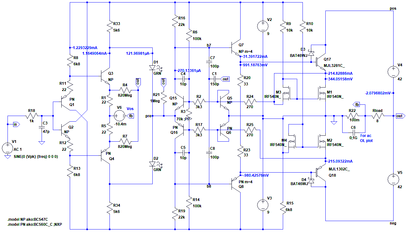
First, use resistors (R8,R33) instead of CCS's for the diamond stage with gain and resistors (R16,R6) for the autobias spreader. Only about 6dB OL gain reduction with resistors (thanks to the +/-9V supply being in bootstrap). I also reduced the diamond current from 5mA to 1mA with a further OL gain reduction of 12dB. So THD is up by 20dB at 1kHz but still acceptable for me -- what counts for me is low enough distortion at 1W and it's fine (since harmonics are of low order, mostly 3rd).
Second, the autobias spreader is driven at the centre (equivalent to the LT1166 driven at the Input pin). Indra1 does this in Post 106. The advantage of driving at the centre is the input stage cannot overdrive the driver transistor when clipping, which means the driver doesn't need current limiting protection when clipping occurs. Two LED's in series combine the two diamond collectors with a current of around 100uA by R8 and R33. R16 is then chosen to give about twice the peak current into the nominal 8 ohm load. Since it is a current drive amplifier a higher peak output current is not deemed necessary.
Third, two BJT diodes are added to the autobias feedback path to limit the voltage to retard the cut-off point of the autobias and this retarding allows a lower idle current. For Class-A (like the autobias F4 in Post 111) the cut-off point of the autobias is not an issue so these extra diodes are not needed. But I was hoping to get autobias idle currents in the 100mA to 200mA range and these extra diodes now allow that bias level. BTW If the autobias loop cuts off there is a sharp gain step near the peak current which is easily heard even if its THD is 0.01% and it is more noticeable than ordinary Class-AB crossover distortion.
Fourth, use Miller-like compensation around the output stage via C1,C7,C8 into the driver bases, trimmed using C1. (The output stage has voltage gain being common emitter with floating supplies). Compensation is chosen to damp ring that appears at clip recovery. Bandwidth is then in the 500kHz to 1MHz range compared to 3-5MHz with the earlier compensation (which used output lead feedback capacitors which are best avoided if possible). I think this heavier (Miller) compensation is a wise move, even though the bandwidth is not as high on paper. Also, heavy Miller compensation makes the amplifier less prone to cable induced instability such as very long speaker cables.
Sim files are attached. The new MOSFET and IGBT versions should appear soon.
Four significant changes to the previous Autobias with MOSdiode and Diamond amp with gain Post 93.
First, use resistors (R8,R33) instead of CCS's for the diamond stage with gain and resistors (R16,R6) for the autobias spreader. Only about 6dB OL gain reduction with resistors (thanks to the +/-9V supply being in bootstrap). I also reduced the diamond current from 5mA to 1mA with a further OL gain reduction of 12dB. So THD is up by 20dB at 1kHz but still acceptable for me -- what counts for me is low enough distortion at 1W and it's fine (since harmonics are of low order, mostly 3rd).
Second, the autobias spreader is driven at the centre (equivalent to the LT1166 driven at the Input pin). Indra1 does this in Post 106. The advantage of driving at the centre is the input stage cannot overdrive the driver transistor when clipping, which means the driver doesn't need current limiting protection when clipping occurs. Two LED's in series combine the two diamond collectors with a current of around 100uA by R8 and R33. R16 is then chosen to give about twice the peak current into the nominal 8 ohm load. Since it is a current drive amplifier a higher peak output current is not deemed necessary.
Third, two BJT diodes are added to the autobias feedback path to limit the voltage to retard the cut-off point of the autobias and this retarding allows a lower idle current. For Class-A (like the autobias F4 in Post 111) the cut-off point of the autobias is not an issue so these extra diodes are not needed. But I was hoping to get autobias idle currents in the 100mA to 200mA range and these extra diodes now allow that bias level. BTW If the autobias loop cuts off there is a sharp gain step near the peak current which is easily heard even if its THD is 0.01% and it is more noticeable than ordinary Class-AB crossover distortion.
Fourth, use Miller-like compensation around the output stage via C1,C7,C8 into the driver bases, trimmed using C1. (The output stage has voltage gain being common emitter with floating supplies). Compensation is chosen to damp ring that appears at clip recovery. Bandwidth is then in the 500kHz to 1MHz range compared to 3-5MHz with the earlier compensation (which used output lead feedback capacitors which are best avoided if possible). I think this heavier (Miller) compensation is a wise move, even though the bandwidth is not as high on paper. Also, heavy Miller compensation makes the amplifier less prone to cable induced instability such as very long speaker cables.
Sim files are attached. The new MOSFET and IGBT versions should appear soon.
Attachments
Last edited:
Here are the sim files for the MOSFET and IGBT versions:
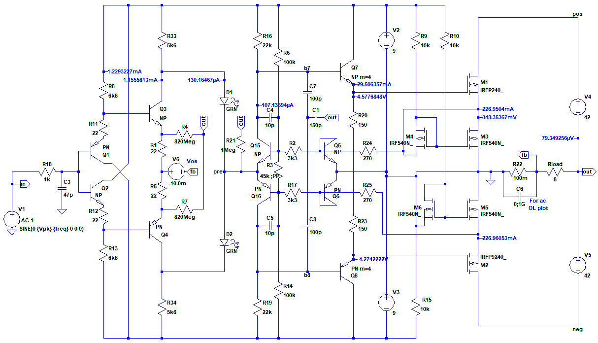
MOSFETs THD at 1W is 0.028% and of low order.
The IGBT version needs heavier compensation due since IGBTs are slower than MOSFETs. V2,V3 increased to 12V due to these IGBT's higher threshold voltage. R3 then set for 220mA idle current. Clip diodes are added to prevent saturation of the IGBT.
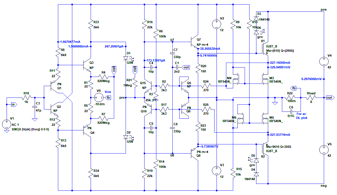
THD is about the same as for the MOSFETs.
MOSFETs THD at 1W is 0.028% and of low order.
The IGBT version needs heavier compensation due since IGBTs are slower than MOSFETs. V2,V3 increased to 12V due to these IGBT's higher threshold voltage. R3 then set for 220mA idle current. Clip diodes are added to prevent saturation of the IGBT.
THD is about the same as for the MOSFETs.
Attachments
The previous post files were not checked for full-power bandwidth and need updating to run at 100kHz (and IGBT version to 40kHz full-power). Files attached. Delete previous ones. Apologies for missing this.
The compensation center node (C7,C8) has been tied to the "pre" node (emitters of the auto-bias spreader). Also the LED's are bypassed with a capacitor and the input stage current doubled to 2mA. C3 input filter has been increased.
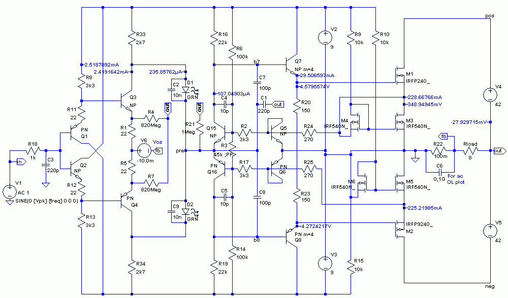
The compensation center node (C7,C8) has been tied to the "pre" node (emitters of the auto-bias spreader). Also the LED's are bypassed with a capacitor and the input stage current doubled to 2mA. C3 input filter has been increased.
Attachments
This shows two variants in one: Differential input and parallel power transistors.
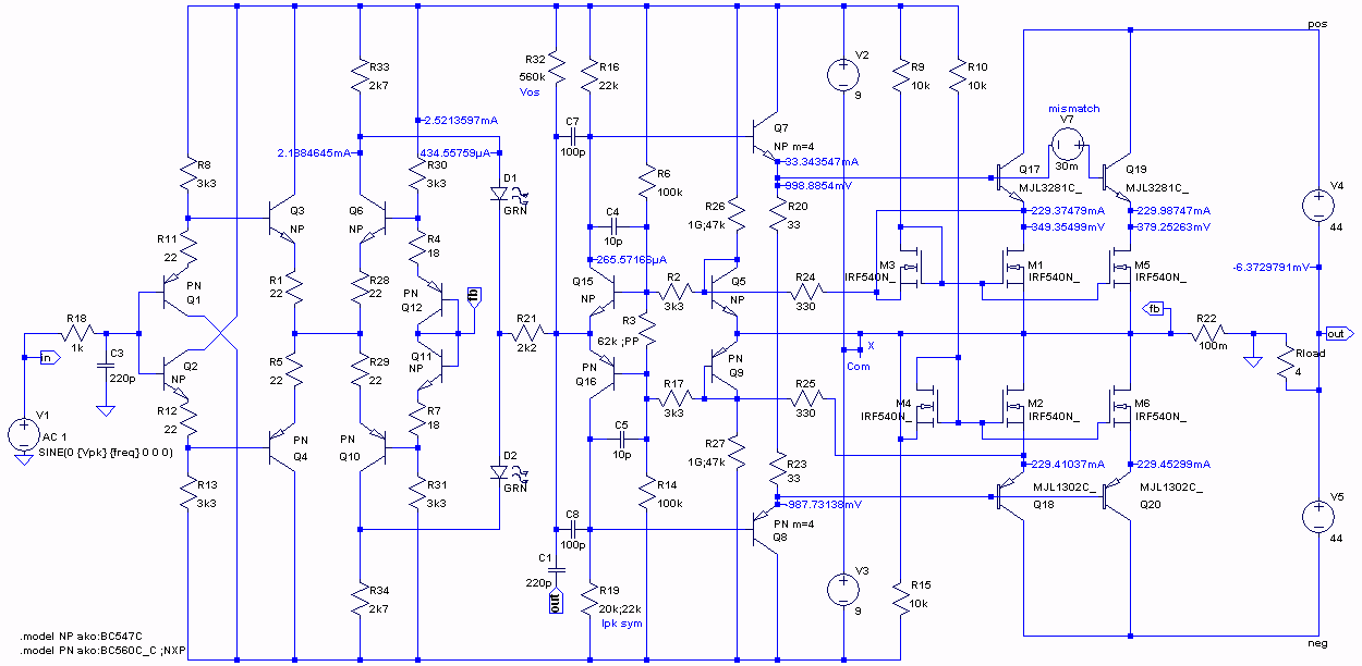
Parallel transistors can drive a 4 ohm load. The 30mV offset for Q19 shows effective current sharing with MOS-diodes for each parallel pair of BJTs. More parallel pairs can be added if the drivers are uprated.
The differential input stage allows feedback from the opposite side of sense resistor R22 so the load can be grounded. (A grounded load allows bridging). The differential stage also allows cancellation of the PNP-NPN difference that otherwise requires a trimpot (or servo) to null out. R4 and R7 are reduced slightly from 22 ohms to 18 ohms to trim the current through the LEDs to around 400uA.
With the load grounded the +/-9V supplies are now floating on the sense signal. An alternative is to break the 9V center ("x") and ground it, this then allows several amplifiers to share the same +/-9V supply. With the center grounded the THD increases slightly.
Another alternative is to change R27,R28 to 47K. This allows the idle current to be reduced to 130mA per pair while maintaining autobias to 10A peak. (Reduce the bias resistor R3 to 47k to get 130mA). THD increases slightly by reducing the idle current to 130mA.
A useful improvement over the previous post is placing R21 (2k2) in series with the input node to the autobias spreader. This improves compensations effectiveness for damping clip recovery. But the beta difference of the PNP and NPN spreaders then causes an offset current that flows through R21 causing the output offset to increase. R32 is added to trim the output voltage as R21 increases due to beta mismatch. Note with R21 around 1k to 2k, capacitors are not longer required across the LEDs.
At full power 200W THD is 0.15% at 1kHz. The open loop gain is 58dB with 9kHz -3dB. Closed loop gain is 30dB, so only 28dB of feedback is used. BTW this is slightly less feedback than present in standard followers. This is design is a very low feedback wideband autobias transconductance amp.
When bridged it gives 400W into 8 ohms. The 8 ohm load connects to each sides "out". Two 44V floating supplies are used. See Post 117.
Here's the 400W bridge with two floating 88V supplies with capacitors. One standard dual secondary transformer runs one channel.

Included in the attached files is a 200W version for 4 ohms using two floating 46V supplies.
Included in the attached files is a 200W version for 4 ohms using two floating 46V supplies.
Attachments
Maybe the last variation is power MOSFET's with Class-G:
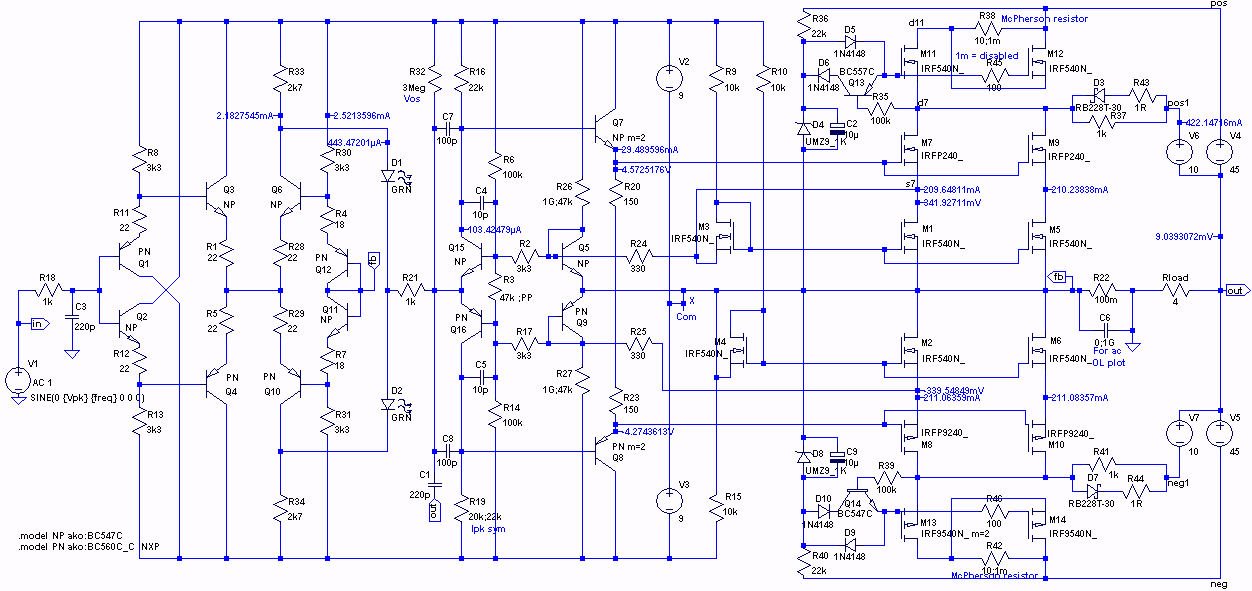
This Class-G includes McPherson resistors (see this post for more). I abbreviate this to "Class-GM". The attached file has a bridge version. The bridge version includes some common mode feedback to keep the two outputs close to 0V.
The single version THD is 0.26% at 180W into 4 ohms and the bridge version is 0.4% at 320W into 8 ohms. At 1W they are 0.03% and 0.01% respectively which is quite adequate for music (being mainly 3rd harmonic distortion up to about 10 watts). With this topology it is easy to scale down the power by reducing the rail voltage, eg a different transformer. Notice the driver and input stages are fed from separate +/-9V so lowering the main supply rails doesn't affect biasing etc. Nice.
Particular care is needed with any Class-G to keep the gain wobbles inaudible. A 1 ohm resistor is added in series with the Schottky diodes to widen the Class-G crossover region so the gain wobbles can then be reduced by nfb.
With added Class-G added the idle dissipation is reduced to about 1/5th. The McPherson resistors then allow the worst case sinewave dissipation to be reduced by about 30% allowing a smaller heatsink. But if the amp is intended only for music (not continuous sinewaves) then the heatsink can be about half that of non-McPherson Class-G Nice😎.
When the single version is run at full output swing (180W/4R) with dual +/-45V rails the heatsink dissipation is 40W and the McPherson resistors are 20W total. This is an efficiency of 75%. Idle heatsink dissipation is only 8W with an idle current of 420mA.
When the single version is run at 1W/4R the heatsink dissipation is only 3.6W with an efficiency of 22%. The idle current can be reduced to 260mA (the minimum for autobias with R26,R27 both 47K and R3 37K) and the efficiency is 30% at 1W which is a typical listening average power with reasonable sensitivity speakers (>90dB/W/m).
These efficiency improvements with Class-GM look quite green🌲 and may swing those who would otherwise go for Class-D.
The main advantages of this topology with Class-GM over Class-D is the wider bandwidth from linear mode and no HF hash on the output or anywhere in the amp enclosure.
Also this topology does not need a lot of negative feedback to get distortion low enough at normal listening power levels like 1W.
A further advantage of this topology is the power MOSFETs provide most of the voltage gain so the driver and input stages can operate at low voltage and don't need any medium-power high voltage fast driver transistors.
Autobias with MOS-diodes (instead of Schottky diodes) is stable with temperature changes and the bias spreader does not need any thermal linkage to any heatsink. The power transistors can be changed from BJT's to MOSFETs without changing the bias settings (only the Locanthi resistor needs changing because MOSFET's have a much higher gate voltage than BJT's).
Most of my variants have been transconductance or current drive but they can also be converted to voltage drive. Current drive reduces speaker intermodulation distortion but needs custom speakers with special attention with damping for the LF driver. Esa Merilainen's peer reviewed paper 'Comparative Measurements on Loudspeaker Distortion: Current vs. Voltage Control' can be download here http://acousticsnew.ippt.gov.pl/index.php/aa/article/download/1780/pdf_255
Attachments
Attached files allow simulation of the Class-GM with a music-like PMR (Peak to Mean Ratio) of 12dB by using a pink noise wav file. The level is set so clipping occurs only once or twice in 100ms. The simulation takes about 20 minutes to simulate 200ms.

The supplied wav file has a 25ms lead-in then 25ms fade-in so I take my average power measurements from 100ms to 200ms.
Average powers are: M7=3.3W, M11=4.1W, M12=9.9W, R38=15.7W, RL=60W. (M7 is the inner MOSFET, M11 the Class-G MOSFET and M12 is the McPherson MOSFET and R38 is the McPherson resistor. Power of M11 is doubled per side.
So heatsink dissipation per side is 2x11+4.1+9.9=36W, so total heatsink dissipation is 72W. Overall efficiency with 60W out and 2x36+2x15.7=103.4W losses (say 105W total with the 0.1 ohm sense resistor and the MOS-diodes) giving 37% efficiency.
Two McPherson resistors dissipate 31.4W total. Without these resistors (standard Class-G) the heatsink dissipation would be 72+31.4=103W so the reduction in heatsink rating is 72/103=0.7 or a 30% reduction with a 12dB PMR music-like signal.
In my previous post I suggested a 50% reduction in heatsink size with music but this simulation suggests a 30% reduction is a more realistic reduction for McPherson Class-G over standard Class-G.
Attachments
Oops😳. Disregard the above calcs and conclusion! My apology. Here's the corrected calcs:
So heatsink dissipation per side is 2x3.3+4.1+9.9=20.6W, so total heatsink dissipation is 41.2W. Overall efficiency with 60W out and (20.6+15.7)=2*36.3=72.6W losses, say 74W total with the 0.1 ohm sense resistor and the MOS-diodes) giving 60/(60+74)=45% efficiency.
Two McPherson resistors dissipate 31.4W total. Without these resistors (standard Class-G) the heatsink dissipation would be 72.6W so the reduction in heatsink rating is 31.4/72.6=0.434 or a 43.4% reduction with a music-like signal.
The reduction in heatsink size with Class-GM over Class-G is close enough to half as a rule of thumb. The actual factor is 57%.
Further sims with a higher PMR giving less clipping and lower average power of 40W gave almost the same reduction factor as above. Also reducing the McPherson resistor from 10 ohms to 5 ohms gave almost the same reduction factor. So the McPherson's improvement appears to be insensitive to the type music PMR and the value of the McPherson resistor (range tested RMph=RL to 2RL).
Please let me know if I still have some errors.
Ian, ref the schematic in #130, for a drop of extra performance, you may want to connect the Q1, Q2, Q11, Q12 collectors to the Q4, Q3, Q6, Q10 emitters respectively. This will create both a linearizing local feedback loop, and also bootstrap the input pairs, so that there is less impact of the evil Early effect.
Probably moot for an open loop amp…
Probably moot for an open loop amp…
Hi Ovidiu,
Thanks for chiming in again after a long break. I hope it is all well l with you and all your adventures.
The Early effect is not much of an issue in the input stage of the amp in Post 130. I'd expect Early effect in diamond follower stages. What I did notice is that Q1 has a higher dissipation the the counterbalancing Q12 (likewise Q2 and Q11) due to the difference in Vce. This may cause a start up (warm up) issue with the difference current through the LED's. I haven't simulated this using electrothermal models so I don't know how much current change there might be at warm up. One way to overcome it is to add resistors with same value as R8 and R13 in series with the collector leads of Q1 and Q2. Then Q3 and Q4 dissipation doesn't match Q6 and Q10 so add resistors of R23 value in their collectors also. I'll check these changes, maybe with some bench tests.
As for this amps topology it is technically a VFA front end with load current sense feedback making it a transconductance power amp. The output stage has an open loop Gm of 20A/V (calculated from the Vpre swing and the output current swing). This gives the power stage an open loop voltage gain of 80 V/V with 4 ohms. The input stage has a voltage gain of about 30. In closed loop the 100 milliohm sense resistor the transconductance is 10A/V giving a closed loop voltage gain of 40. This means there's only about 36dB of feedback around the amp.
Earlier versions had input stages with higher gain by using 4 CCS's (8 transistors extra). Later versions therefore have higher THDs. Another reason for higher THD in the latest versions is the use of BJT trans-diodes in the feedback path for the autobias. They increase THD by 2-4 times but lower the minimum idle current needed for the autobias loop to stay active over the entire output current range. The diodes also allow higher RDSon MOS-diodes to sense the output MOSFETs current for the autobias transistors. With these transdiodes the RDSon can be about 10 times higher (but as mentioned sacrificing THD). My preference would be to use very low RDSon MOS-diodes and not use the transdiodes since very low RDSon low voltage MOSFETs (5mR/25V) cost no more than the IRF540N's (50mR/100V) that I use in Post 130.
I hope that fills in a few more details. Thanks again for your feedback.
Cheers, Ian
Hi All,
At last, some bench testing of the autobias control loop using MOS-diodes. Starting with the basic circuit below.
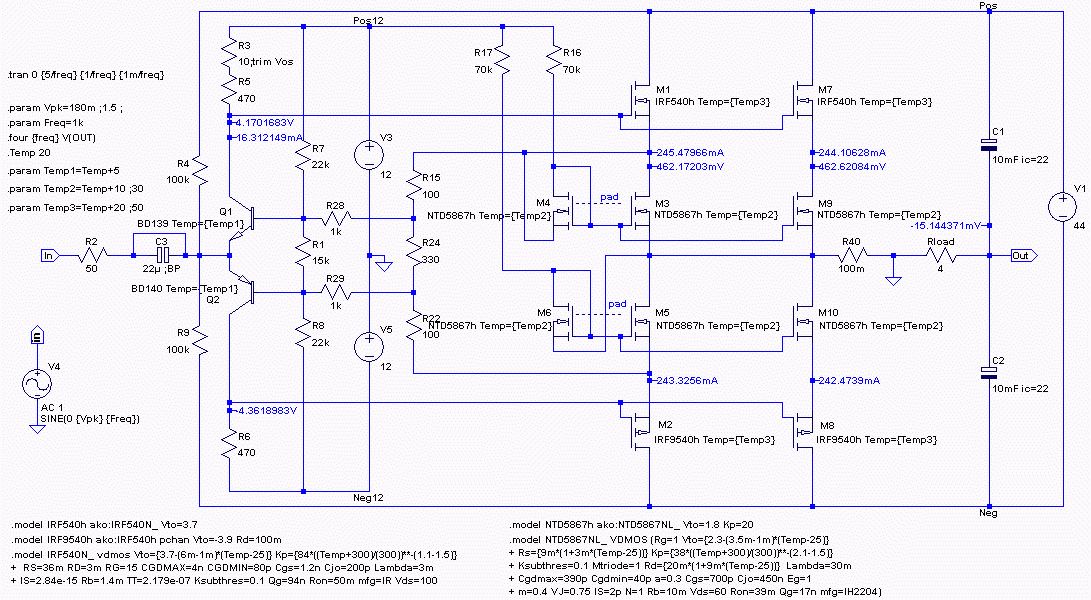
The thermal stability has been confirmed😃. And linearity is as simulated (files attached).
I used IRF540/9540 for the main MOSFETs and NTD5867 MOSFETs for the MOS-diodes (40mR 60V IPAK). The spreader BJT's are BD139/140's operating at 16mA. The power supply is floating and is split using two 10mF capacitors to the load. The 0.1 ohm current sensing resistor provides some local degeneration and is used for feedback to an input stage for a practical transconductance amplifier. This is just the power stage.
Apart from linearity (ie distortion) I checked thermal behaviour. Two cases: 1) from turn on with no signal as it warms up. 2) The idle current change as it cools down after running hot at full power. These bench tests have been necessary because the simulations lacked accurate time constants temp-cos for the MOSFET models.
1) At turn on there is a thermal transient - starting at 600mA and falling to a steady 400mA after about 30 seconds. This transient is caused mainly by the BJT autobias transistors warming up by about 5 degrees C.
To work out if it is the BJTs warming up I used a hot air gun to warm the BJT autobias transistors (maybe 10-15C) before turning on the amps power. At turn on idle current was down to 150mA, returning to 400mA as they cooled down and the rest of the amp warmed up.
This thermal effect can be eliminated if driver transistors are used so the spreader transistors can operate at a low current (eg <0.5mA). But even if this heating transient is removed there is still a large change in idle current with ambient temperature variations. One solution is to make R1 or R24 change with ambient temperature using a thermistor (and thermally couple it to the spreader transistors).
2) Now the idle current change after running at full power. I tried two arrangements for thermal coupling of the 2 MOS-diodes: M3 is coupled to M4. Also M5 to M6.
My first test used a thin thermal pad between M3-M4 & M5-M6. The pad was made from plumbers thread tape. I found two layers were needed to stop shorting when they were clamped tight.
With the thin pads the idle current dropped from 400mA to about 200mA after operating at full power for 5 minutes. This gives over-compensation.
My second test was with a normal thermal pad between M3-M4 & M5-M6. This reduced the idle current after running hot to 350mA after heating up at full power. The thicker pad provides some needed thermal attenuation since the temp-co of M4 and M6 are too high. It appears operating M4 at a relatively low bias current (0.1mA) gives a significantly higher temp-co than its partner MOSFET (M4) which runs at a much higher current, the idle current of 200mA for each pair.
Linearity.
I didn't have a distortion meter handy so I used my scope on X-Y to check linearity. It showed the simulation was very close to my circuit. The simulation gain was higher than my circuit and this was probably due to resistance in thin hook-up wire and breadboard contact resistance. The FFT plot from a simulation (below) is a good indication of my test circuit 0.2% at 1W into 4 ohms, 400mA bias.
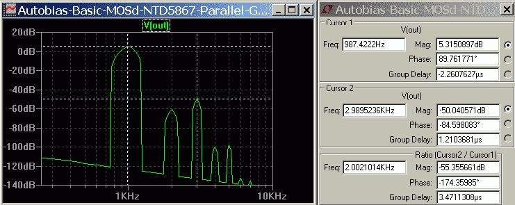
Measured voltage gain was x19 so Gm is about 5A/V. This output stage would make a simple no-feedback current drive guitar amp! Or a Zen amp! (It can be driven by an opamp with about 10mA peak and 1V peak).
This autobias control loop using MOS-diodes is novel as far as I am aware. Please let me know if it has been mentioned anywhere else other than diyAudio™️.
Summary of tests so far:
1) Autobias with MOS-diodes and no source resistors is thermally stable. The idle current for best linearity using relatively low RDSon MOSFETs for the MOS-diodes is quite high without source resistors (400mA with 44V is 18 watts for 25W output).
2) Paralleling of output stages is also stable without any source resistors.
3) No problematic thermal transients from the MOS-diodes heating and cooling as the output power changes. (The thermal transient in the spreader BJT's is a separate issue not related to output power variation). The thermal coupling of the MOS-diode MOSFETs needs to be chosen correctly to prevent overcompensation.
4. One downside: there is a sharp recovery from hard clipping that sounds bad😰! At least that's for the output stage only with no feedback. I'm not sure how (or if) this can be eliminated apart from limiting the drive to the output stage so it cannot enter hard clipping, eg, back-back LED diodes in the input(?). It's like Bob Cordell has said, "pick your poison".
More tests soon.
Cheers,
Ian Hegglun
At last, some bench testing of the autobias control loop using MOS-diodes. Starting with the basic circuit below.
The thermal stability has been confirmed😃. And linearity is as simulated (files attached).
I used IRF540/9540 for the main MOSFETs and NTD5867 MOSFETs for the MOS-diodes (40mR 60V IPAK). The spreader BJT's are BD139/140's operating at 16mA. The power supply is floating and is split using two 10mF capacitors to the load. The 0.1 ohm current sensing resistor provides some local degeneration and is used for feedback to an input stage for a practical transconductance amplifier. This is just the power stage.
Apart from linearity (ie distortion) I checked thermal behaviour. Two cases: 1) from turn on with no signal as it warms up. 2) The idle current change as it cools down after running hot at full power. These bench tests have been necessary because the simulations lacked accurate time constants temp-cos for the MOSFET models.
1) At turn on there is a thermal transient - starting at 600mA and falling to a steady 400mA after about 30 seconds. This transient is caused mainly by the BJT autobias transistors warming up by about 5 degrees C.
To work out if it is the BJTs warming up I used a hot air gun to warm the BJT autobias transistors (maybe 10-15C) before turning on the amps power. At turn on idle current was down to 150mA, returning to 400mA as they cooled down and the rest of the amp warmed up.
This thermal effect can be eliminated if driver transistors are used so the spreader transistors can operate at a low current (eg <0.5mA). But even if this heating transient is removed there is still a large change in idle current with ambient temperature variations. One solution is to make R1 or R24 change with ambient temperature using a thermistor (and thermally couple it to the spreader transistors).
2) Now the idle current change after running at full power. I tried two arrangements for thermal coupling of the 2 MOS-diodes: M3 is coupled to M4. Also M5 to M6.
My first test used a thin thermal pad between M3-M4 & M5-M6. The pad was made from plumbers thread tape. I found two layers were needed to stop shorting when they were clamped tight.
With the thin pads the idle current dropped from 400mA to about 200mA after operating at full power for 5 minutes. This gives over-compensation.
My second test was with a normal thermal pad between M3-M4 & M5-M6. This reduced the idle current after running hot to 350mA after heating up at full power. The thicker pad provides some needed thermal attenuation since the temp-co of M4 and M6 are too high. It appears operating M4 at a relatively low bias current (0.1mA) gives a significantly higher temp-co than its partner MOSFET (M4) which runs at a much higher current, the idle current of 200mA for each pair.
Linearity.
I didn't have a distortion meter handy so I used my scope on X-Y to check linearity. It showed the simulation was very close to my circuit. The simulation gain was higher than my circuit and this was probably due to resistance in thin hook-up wire and breadboard contact resistance. The FFT plot from a simulation (below) is a good indication of my test circuit 0.2% at 1W into 4 ohms, 400mA bias.
Measured voltage gain was x19 so Gm is about 5A/V. This output stage would make a simple no-feedback current drive guitar amp! Or a Zen amp! (It can be driven by an opamp with about 10mA peak and 1V peak).
This autobias control loop using MOS-diodes is novel as far as I am aware. Please let me know if it has been mentioned anywhere else other than diyAudio™️.
Summary of tests so far:
1) Autobias with MOS-diodes and no source resistors is thermally stable. The idle current for best linearity using relatively low RDSon MOSFETs for the MOS-diodes is quite high without source resistors (400mA with 44V is 18 watts for 25W output).
2) Paralleling of output stages is also stable without any source resistors.
3) No problematic thermal transients from the MOS-diodes heating and cooling as the output power changes. (The thermal transient in the spreader BJT's is a separate issue not related to output power variation). The thermal coupling of the MOS-diode MOSFETs needs to be chosen correctly to prevent overcompensation.
4. One downside: there is a sharp recovery from hard clipping that sounds bad😰! At least that's for the output stage only with no feedback. I'm not sure how (or if) this can be eliminated apart from limiting the drive to the output stage so it cannot enter hard clipping, eg, back-back LED diodes in the input(?). It's like Bob Cordell has said, "pick your poison".
More tests soon.
Cheers,
Ian Hegglun
Attachments
Last edited:
Hi All,
My tests in Post 135 gave higher volt drops across the MOS-diodes than in simulations. Sims show 460mV at 240mA but my bench version was twice that 800mV. I haven't found why. It must be the MOSFET models need changing somehow. It is a concern because the MOS-diodes dissipate more power than I expected from my sims.
So I bench checked the alternative of using Schottky diodes (like Post 90) where the autobias spreader has no base-collector resistors like a Vbe multiplier does. This means the Schottky diodes are now fully within the autobias feedback loop. Since the Schottky diode temp-co is negative (opposite to MOS-diodes) the Schottky diodes must be thermally linked to the spreaders to prevent thermal runaway. My basic test rig is shown below:
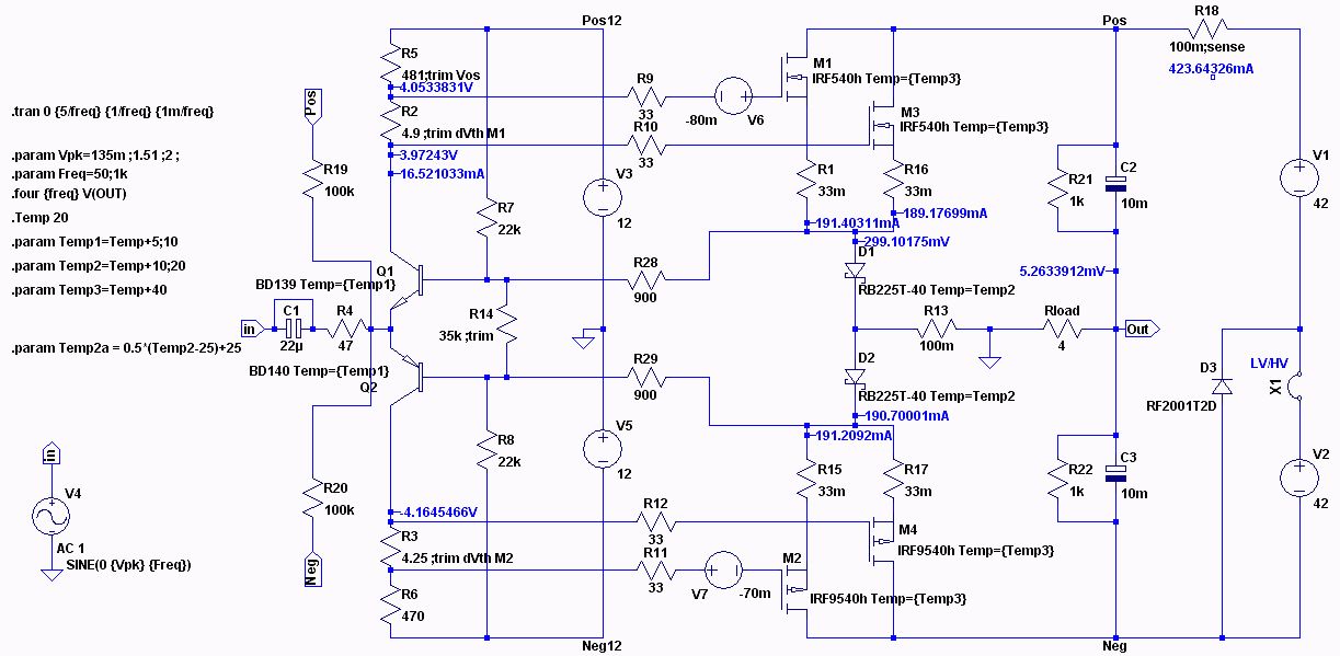
The Schottky diodes I used are TO-220 STPS1045. The MOSFETs operate in parallel with one Schottky diode per pair of MOSFETs to test if this is thermally stable. I found 33mR sharing resistors were needed when the voltage was 84V (but not for 42V). R2 and R3 are 10R trimpots to allow trim currents in the paralleled MOSFETs. Threshold voltage differences of up to 150mV can be trimmed out for M1 and M3 by placing a meter between sources of M1 and M3 (likewise M2 & M4).
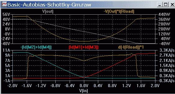
I found an idle current of 400mA gave quite good linearity. Thermally linking the spreaders Q1 and Q2 to the Schottky's with standard thermal washers gave over-compensation (the idle current halved after running at 7A peak for a while). The spreaders and Schottky's were mounted separately to the main heatsink. Changing to a 1mm fibre-glass PCB washer to reduce the compensation, when run with 7A peaks for a few minutes the Schottky-spreaders warmed up, and then with no signal the idle current fell to 320mA after about 1 minute, rising slowly back to the original 400mA after 30 minutes.
This seems to be a satisfactory thermal arrangement for the power stage of an amplifier.
The voltage gain and Gm with Schottky diodes are about 2 times higher than with IRF540N MOS-diodes, and the optimum idle current is no higher than IRF540N MOS-diodes. My attached simulation suggests THD is 0.5% at 1W into 4 ohms, 400mA bias but double Gm; about the same as the previous tests with MOS-diodes for the same gain.
I think I prefer the Schottky version with less MOSFETs to wire up.
My tests in Post 135 gave higher volt drops across the MOS-diodes than in simulations. Sims show 460mV at 240mA but my bench version was twice that 800mV. I haven't found why. It must be the MOSFET models need changing somehow. It is a concern because the MOS-diodes dissipate more power than I expected from my sims.
So I bench checked the alternative of using Schottky diodes (like Post 90) where the autobias spreader has no base-collector resistors like a Vbe multiplier does. This means the Schottky diodes are now fully within the autobias feedback loop. Since the Schottky diode temp-co is negative (opposite to MOS-diodes) the Schottky diodes must be thermally linked to the spreaders to prevent thermal runaway. My basic test rig is shown below:
The Schottky diodes I used are TO-220 STPS1045. The MOSFETs operate in parallel with one Schottky diode per pair of MOSFETs to test if this is thermally stable. I found 33mR sharing resistors were needed when the voltage was 84V (but not for 42V). R2 and R3 are 10R trimpots to allow trim currents in the paralleled MOSFETs. Threshold voltage differences of up to 150mV can be trimmed out for M1 and M3 by placing a meter between sources of M1 and M3 (likewise M2 & M4).
I found an idle current of 400mA gave quite good linearity. Thermally linking the spreaders Q1 and Q2 to the Schottky's with standard thermal washers gave over-compensation (the idle current halved after running at 7A peak for a while). The spreaders and Schottky's were mounted separately to the main heatsink. Changing to a 1mm fibre-glass PCB washer to reduce the compensation, when run with 7A peaks for a few minutes the Schottky-spreaders warmed up, and then with no signal the idle current fell to 320mA after about 1 minute, rising slowly back to the original 400mA after 30 minutes.
This seems to be a satisfactory thermal arrangement for the power stage of an amplifier.
The voltage gain and Gm with Schottky diodes are about 2 times higher than with IRF540N MOS-diodes, and the optimum idle current is no higher than IRF540N MOS-diodes. My attached simulation suggests THD is 0.5% at 1W into 4 ohms, 400mA bias but double Gm; about the same as the previous tests with MOS-diodes for the same gain.
I think I prefer the Schottky version with less MOSFETs to wire up.
Attachments
Last edited:
My last post using Schottky diodes rather than MOS-diodes for current sensing required sharing resistors to stop current hogging. I'd like to avoid source resistors so I tried paralleling two "slices" like the LT1166 application note recommends for paralleling. Two identical power stages are run in parallel each with their own autobias generator and Schottky diodes.
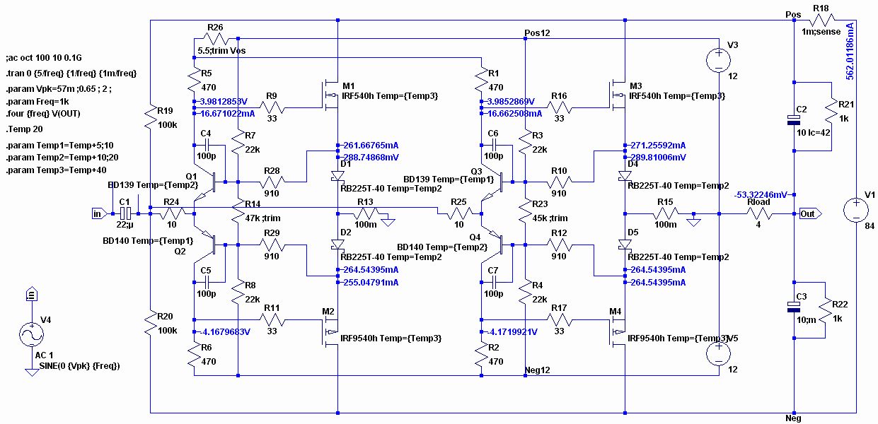
This works well and provides good current sharing and does not need matching of MOSFET's. This makes the few extra components worthwhile.
The idle current for good linearity is 500mA or about 50W for a 200W amp. Idle current can be run at 300mA but then you need about twice as much feedback to get the same linearity - so there is a trade off. BTW it is known that the current for optimum bias for a Class-AB stage increases as the source resistance is reduced - so don't be too upset that this stage with no added source resistance requires quite a high idle current to get the best linearity. What you get in exchange for this extra heat is a wider Class-A band (slightly more than the 1W average needed with good sensitivity speakers) and plenty of voltage gain as well (which means you can now use low voltage opamps or low voltage discrete driver stages). Also the power stage PCB can be smaller and run cooler without the usual hot source resistors.
There are now no source resistors only the local feedback resistors R13, R15 which can be 2W MF. The Gm with 500mA bias is 15A/V with the local feedback resistors giving a voltage gain of 62 into 4 ohms, requiring only about 450mV input to get full output swing of 28V into 4 ohms.
The last test will be the short circuit output test with full output to see if the SOA can withstand it for a short time (until a thermal cut-out trips). Maybe 3 slices are needed to withstand the output short test? Some simulations would help to decide.
Another development is the thermal feedback from the Schottky's to the autobias spreaders. Q1 and Q3 are mounted on the Schottky's and Q2, Q3 are left at ambient. This halves the effective temp.co for the spreader and about the required compensation as the Schottky's heat up (from turn on and then when run at full power). The BD139-140 packages were mounted on the top end of the TO-220 Schotty's metal tab with a thermal washer, and two TO-220's were mounted on a small metal plate (2cmx3cm) separate from the main heatsink. The response time was quite fast with a slight undershoot after running hot. Using only one spreader transistor for compensation per slice worked much better than using a PCB thermal washer to drop the temperature from the Schottky's which created a huge undershoot after running at full power.
Another finding is the IRF540N is less robust than the original IRF540, so I will not be using IRF540N's after I restock. The IRF9540N may be OK together with the older IRF540 but I need to do more tests to see if I can still use the IRF9540N's in these amps.
Attachments
Last edited:
Further bench tests with parallel slices. Now with older IRF540 and IRF9540.
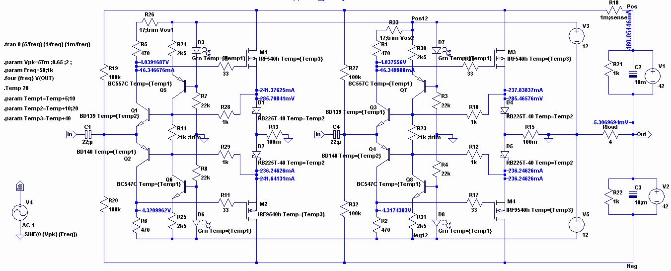
CCS's are used to prevent MOSFETs blowing at power down. My bench test 12V supply is derived from the same transformer as the main rails and when I turn off the transformer the 12V rails collapse faster than the main rail supply causing a large idle current that blows the MOSFETs when run with 84V -- it was not a problem on 42V total (+/-21V). When the 12V rails collapse current through R3,R4, R7 and R8 (of previous post) fall, the idle current increases. The idle current increases by 500mA with a 1V drop in the 12V rail voltage for the previous arrangement.
Replacing these resistors with CCS's the idle current reduces by 100mA with a 0.6V drop in the 12V rail voltage which allows the 12V rails to safely allow the 12V rails to collapse before the main rails. I think these CCS's are needed to bullet proof autobias.
Another variation from the previous circuit is to trim the output offset voltage independently for each section. This was done by disabling the other section by shorting the two collectors of the autobias spreader transistors. Also the inputs for each section has a capacitor to prevent interaction while trimming. If the capacitors are omitted then it is possible to get "tensioning" current flowing between the two MOSFET sections -- like DoubleCross -- but I haven't looked into whether this is useful with autobias.
More tests on idle current change at turn on from cold and after running at full power with only one of the autobias spreaders coupled to the Schottky diodes and the other spreader transistor at ambient. At turn on the idle current is set for 550mA total which quickly stabilizes to 530mA after 30 seconds, then a slower fall to 505mA after 5 minutes. Running at full output into 4 ohms for 15 minutes the idle current is 530mA at turn off of signal, falling to 503mA after 15 seconds and stays there while cooling back to normal.
This is the best thermal stability result so far and concludes my quest for a stable autobias power stage that can be paralleled without needing to match any of the MOSFETs.
BTW the simulation in the previous post took a long time to start and this was due to the 84V supply splitting into half with resistors. Replacing the 84V supply with two 42V sources solves this (software) start up problem. So the attached file has two 42V sources to get the circuit to run fast. But my bench rig has one 84V supply that is split with resistors.
Attachments
Hi Ian,Hi All,
Four significant changes to the previous Autobias with MOSdiode and Diamond amp with gain Post 93.
Great job on these simulations! I have tried your files https://www.diyaudio.com/community/attachments/diamond-autobias-mosdiode-mjl3281-gm-zip.1032112/ and got distortion as follows
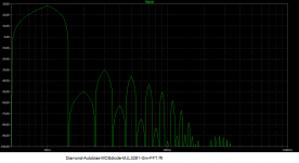
that is about 0.13% THD at 1kHz. Is it OK, or did I make a mistake? I would consider such distortion a bit high, to think about building a prototype. Just to add, I would not consider MOSFETs or IGBTs output devices, just BJTs.
- Home
- Amplifiers
- Solid State
- Towards a wideband non switching Auto Bias power amp