I have tested that circuit, however it is not working good. Is is working good only when it is not overexcited. When there is just a little overexciting the disortion of the "D resetted channel" is too high.
So i decided to make another circuit. The third TL494 is working just like pulse-generator for the D flip flop. The inverted outpus of TL494 number 1 and 2 are here because of the inverted maximum duty cycle 95% -> it makes minimum 5% duty cycle. So the current through the plasma never goes zero - no sizzling of the plasma. However i have BIG problems with disruptions from GDT. The D flip flop is working correctly until I attach the gate driving tranformers. When i put them in the circuit they are making spikes and the D flip flo stop working correctly. It doesn't alternate the pulses! The input is on the output! So the frequency is doubled and that is really not good 🙁 Is any defence agains this?
So i decided to make another circuit. The third TL494 is working just like pulse-generator for the D flip flop. The inverted outpus of TL494 number 1 and 2 are here because of the inverted maximum duty cycle 95% -> it makes minimum 5% duty cycle. So the current through the plasma never goes zero - no sizzling of the plasma. However i have BIG problems with disruptions from GDT. The D flip flop is working correctly until I attach the gate driving tranformers. When i put them in the circuit they are making spikes and the D flip flo stop working correctly. It doesn't alternate the pulses! The input is on the output! So the frequency is doubled and that is really not good 🙁 Is any defence agains this?
Attachments
Last edited:
Are the +5V rails decoupled near the ICs? Are you using F TTL or CMOS? Are digital circuits placed away from the drivers, MOSFETs and the txfmr?
There must be a lot of flux being cut in the windings. I once had a simple CMOS switching amplifier drawing lines on my TV screen!
Is your GDT making lot of EMI......?
There must be a lot of flux being cut in the windings. I once had a simple CMOS switching amplifier drawing lines on my TV screen!
Is your GDT making lot of EMI......?
The capacitors are as near as possible to the ICs. Using F TTL. Yes, there is a lot of flux in the windings about 0.4A altogether. The windings are 1/1.5/1.5 twisted trifilar. I have connected the grounds on the breadboard in bottom, middle and top of the board and it magically worked for 40kHz - with two plasma arcs running! I will have to make a PCB for it. Do you have any tips for it? Double-layer - top power + signal, bottom spilled GND?
Dont think. Go double layer.
Bottom = ground filled plane (maybe interrupted at places if required with no probs).
Use double layer even if you re forced to use through hole components (due to any reason)
Since this is an open-loop system, you re not likely to have problems even on a breadboard, but changing to PCB will show evident differences in performance.
Try to reduce the physical area occupied by the circuit to a minimum. I think it will be wise to place the 'power' items (MOSFETs, and GDT) away from the others. Try to get the MOSFETs' heatsink (grounded) to act as a shield between the controller and power sides.
A shield (grounded) may also be needed between the L&R channels, if the crosstalk is not satisfactory.
All the Best.
Last edited:
Well, i'm will have to use THC. But the ICs have pins solderable only on the bottom side. Will it matter if use the top ground filled? Or put them on the other side?
Well, i would prefer to bend (or cut) the leads of the IC (or socket) and keep the ground plane below as routing is easier (you dont have to mirror prior to printing).
This way I ll be able to keep the shielding due to the ground plane (bottom) and screens on the upper side.
I dont think its a problem if you have the patience to try out both ways! 🙂
This way I ll be able to keep the shielding due to the ground plane (bottom) and screens on the upper side.
I dont think its a problem if you have the patience to try out both ways! 🙂
Why do you needed to use two TL494's at all? 😕
Why do you put left and right channel signals into single channel plasma speaker? 😕
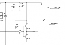
My suggestion is to use the single TL494 (it's output flip-flop has strong opposite pulses), feeding already mixed left and right channel signals to it.
Please, see attached pic.
Why do you put left and right channel signals into single channel plasma speaker? 😕
My suggestion is to use the single TL494 (it's output flip-flop has strong opposite pulses), feeding already mixed left and right channel signals to it.
Please, see attached pic.
Attachments
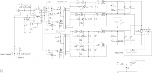
I'm not putting left and right channels into a single speaker. I have two HV transformers 🙂 I thought it's easy to recognise, but now i see it's not recognisable 🙁
I'm alternating the pulses because the voltage spikes from two paralel coils at one time cannot be handled by the transistors. I've tried that, the transistors blew after a short time.
I'm alternating the pulses because the voltage spikes from two paralel coils at one time cannot be handled by the transistors. I've tried that, the transistors blew after a short time.
I'm not putting left and right channels into a single speaker. I have two HV transformers 🙂 I thought it's easy to recognise, but now i see it's not recognisable 🙁
I'm alternating the pulses because the voltage spikes from two paralel coils at one time cannot be handled by the transistors. I've tried that, the transistors blew after a short time.
As I understand, these two HV transformers are connected to a SINGLE 'plasma tweeter', right? So why do you need to drive a single tweeter with two different signals from left and right channels?
... the voltage spikes from two paralel coils at one time
Then I do not understand, which two parallel coils do you mean? 🙁 Do you mean the secondary windings of GDT1/GDT2?
The high current spikes in your half bridges can occur only because of too high switching frequency, I think. Too high frequency can occur because of some undesired feedback coupling (between arc and TL494 because of EMI, for example).
Well, when the two HV coils are turned off in one time, each of them generates a spike. The spikes are summed on the two paralel capacitors. At first, this is generating doubled EMI (maybe that was reason why transistors blew), at second the power that is taken pulsed and the rippling is not good.
Well, when the two HV coils are turned off in one time, each of them generates a spike. The spikes are summed on the two paralel capacitors. At first, this is generating doubled EMI (maybe that was reason why transistors blew), at second the power that is taken pulsed and the rippling is not good.
At turn off time, the spikes from primary coils are handled by MUR diodes (like in usual inductive switching). Transistors take no action at all in this moment, so generally they cannot be damaged because of these spikes, I would think. Also, these spikes cannot charge your two parallel 470uF capacitors much...
I would simply try to shield your modulator part with some ground screen or metal enclosure, since 25KV arcs (maybe event higher in your schematic) is not a joke and can disturb anything around pair of meters... 🙂
Yes man, the loop can close in somewhere because anything between the mosfets and tweeter (both inclusive) can be a potential EMI source. [Please remember that even the ignition systems in vehicles cause a lot of man-made EMI/RFI] Coils with lot of flux rate are great villains.
Even I think you need to separate (strictly) your "power" and "no-power" areas.
If you still have problems, i think you must go for RF PCB design strategies (such as double ground plane or ground / power plane with sealed metallic enclosure etc.)
Even I think you need to separate (strictly) your "power" and "no-power" areas.
If you still have problems, i think you must go for RF PCB design strategies (such as double ground plane or ground / power plane with sealed metallic enclosure etc.)
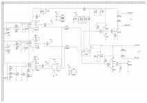
I have designed a prototype. The protected area in top right corner is the power section with mosfets. U6 is the open collector inverter. U5 NAND gate and U4 the most problematic thing - D flip-flop. There is one bridge +12V to power up the TL494s. I hope this should be enough to make it run properly.
Attachments
Xkrik, I like your design and have always wanted to build plasma tweeters, thanks for this!
Just my two cents on your gate drive: You may want to increase R17 and R18 (connecting the 1k to ground BEFORE them), I think you can safely go up to 100 Ohm. This should give you a softer switching on the primary side, and reduce the stress on all components. If you can measure the temperature on the IRF530's, increase slowly until they start getting more hot than usual.
On the gate drive on the secondary side (the 600V MOSFETs), you can increase those resistors (R22, R26, R30, R34) too, making the switching softer, and you should make sure to make the loop (gate transformer - resistor - gate - source - transformer) as small and short as possible. These HV MOSFETs can switch very fast and very hard, and that may cause some trouble in your circuit. Check the switching waveforms across the transistors, when you increase the resistors the spikes should become smaller.
Also, I noticed you are driving both channels from the same power supply cap, you may want to add a little LCL filter between this cap and each channel, to isolate the two from each other. This can be small, e.g. 1/10 of your switching frequency. That should help with the switching transients influencing each other - if the two channels are quite close, and the power supply cap far away, a lot of "local" current will flow and that may cause the transistors to fail
hope that helps!
I thought it too, but i have found that is better to always send some pulse ( no zero pulses ) to HV transformer. Because the plasma arc will never stop. This is done by inverting pulses from TL494 (making maximum 95% duty into 5% minimal duty). If you know how to do it by using just two TL494 (or by single one) show us. The third TL494 is just for making synchronization pulses for D flip-flop and other two TL494. Yes, it is possible to do it without using another D-flip flop (using internal TL494) but the 95% duty was making problems.I still think, that it is possible to implement it using only two TL494 ICs, but if you like this complexity, then ok 😉
Anyway, I would suggest to simplify/improove your drivers schematic slightly. Please, see attached pic.
Yes, i thought about the capacitor in series with the GDT. In the first schematic i tried to use it, but it was not working, because the capacitor never discharges, so I threw that away.
hesener:
IRF's (low voltage side) never go hot, they are cold like other components. The goings on 600V transistors are little bit overshooted on beginning. About 3-4 volts above normal line. But it's working fine a these transistors are nicely warm after 45minutes of testing. It looks like they even don't need heatsink.
However the loops on secondary side are BIG. I didn't know anythink about designing PCBs when I was designing it. But it work's 🙂
I attach multisim data of it.
Attachments
Last edited:
OK - thats good. nevertheless, in order to reduce the noise on the gate and high voltage side (that can and will cause high spikes) it might be good to slow switching down a little bit, with higher gate resistors , you should see much "nicer" square waves. And, think about the little LCL filter between the two channels, it should improve reliability and also soundstaging, through better channel separation.....
- Status
- Not open for further replies.
- Home
- Amplifiers
- Class D
- TL494 based plasma tweeter