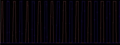
I've been simulating it, but i didn't get anything 🙁 Your attached image is just that what I've got. 0,66 channel has wider pulses and the 0,33 has narrower pulses. But I still don't get why this could be useful...
And yes i want them interleaved (Maybe the word asynchronous was not good)
And yes i want them interleaved (Maybe the word asynchronous was not good)
Last edited:
Dont you find these pulses interleaved in time?
Also reduce the amplitude of your inputs so that they re below 0.33*vcc.
Or take this:
Left channel = 0.4V sine wave + 0.5 V DC
Right channel = 0.4V sine wave - 0.5 V DC (note the sign)
Ramp = +/- 0.5 V
If you dont get something like this below then invert one of the PWMs.
Also reduce the amplitude of your inputs so that they re below 0.33*vcc.
Or take this:
Left channel = 0.4V sine wave + 0.5 V DC
Right channel = 0.4V sine wave - 0.5 V DC (note the sign)
Ramp = +/- 0.5 V
If you dont get something like this below then invert one of the PWMs.
Attachments
Last edited:
Why? Just paste your output here.
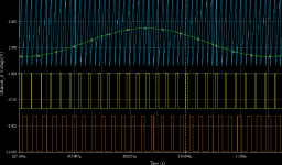
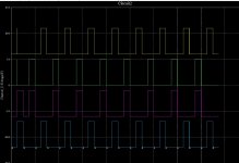
And #22 is what is meant by interleaving pulses. The 0.66 channel that has wider pulses should br inverted
Isnt it what you want?
And #22 is what is meant by interleaving pulses. The 0.66 channel that has wider pulses should br inverted
Isnt it what you want?
Last edited:
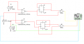
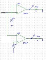
1) You dont need any flip flops, just take the output from the comparators.
2) Exchange +/- inputs of U2 and change input phase from 180 to 0 degrees.
3) Dont use DC on the sawtooth.
The circuit and corresponding output shall look like this:
2) Exchange +/- inputs of U2 and change input phase from 180 to 0 degrees.
3) Dont use DC on the sawtooth.
The circuit and corresponding output shall look like this:
Attachments
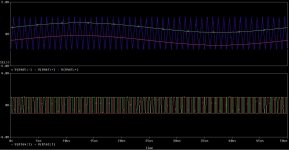
Well, i though that i was something quite different 🙂 I was still thinking about another schematics. However, for proper function of this i have guarantee that sinus won't overlap the triangle on both sides of voltage.
That is exactly why the DC offsets of 0.66*Vcc and 0.33*Vcc used. These separate the sinusoids vertically so that they dont overlap even if they re completely out of phase. i.e. left = negative of right (worst case)
This non-overlap will guarantee non-overlapping pulses at the PWM outputs.
All the Best.
This non-overlap will guarantee non-overlapping pulses at the PWM outputs.
All the Best.
Last edited:
Thanks, but how to limit the pulses to 50% ? If signal exceeds the sawtooth for more than a period it is not safe to switch on the transformer for so long time. So it must be limited. The flip-flop will take it like a single pulse and won't flip it. 🙁
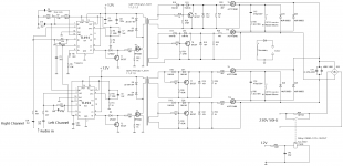
First, what type of converter are you trying to build?
For now it looks like 2switch flyback without rectifier with gates driven by small forward transformer, right?
For now it looks like 2switch flyback without rectifier with gates driven by small forward transformer, right?
It's not exactly a converter. I'm using the transformer not like standard flyback - no energy pumping to secondary. The energy is directly transformed into secondary. Then the high-voltage breaks air and makes plasma. Because there is no load on secondary when the transformer is switched off I'm using the recuperation diodes. I forgot to show winding dots and the diode, because this section works fine. There are two HV-transformers.
Edit:
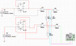
I've have just figured out what i wanted. This won't allow pulses that aren't alternated.
Edit:
I've have just figured out what i wanted. This won't allow pulses that aren't alternated.
Attachments
Last edited:
Oh, you re quite a digital guy!!!!!!!!!!! And I was trying to give you analogue solutions......... 🙂
The circuit looks like the phase-frequency detector inside 74HC4046. 🙂
Dont forget to account for the delay of the AND gate. Use the fastest of devices (74F,74AHC) etc to obtain the least disturbing hazards.
Dont forget to account for the delay of the AND gate. Use the fastest of devices (74F,74AHC) etc to obtain the least disturbing hazards.
Ok, thanks 🙂 From the TTL logic how to drive the IRF530 (T3 and T4)?
Hope tomorrow (+24hours from now) I will have components and I'll test it.
Hope tomorrow (+24hours from now) I will have components and I'll test it.
Xkrik, I meant the delay of the U9.
You may use High voltage 4000 series CMOS to get 12V output but for the delay (very many nanoseconds).
From TTL, you need to shift to the 12V levels (pls lookup TTL-CMOS interfacing) using discrete ckts and then apply emitter follower as before.
http://www.fairchildsemi.com/an/AN/AN-314.pdf
You may use High voltage 4000 series CMOS to get 12V output but for the delay (very many nanoseconds).
From TTL, you need to shift to the 12V levels (pls lookup TTL-CMOS interfacing) using discrete ckts and then apply emitter follower as before.
http://www.fairchildsemi.com/an/AN/AN-314.pdf
Last edited:
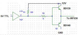
Use an open collector buffer to get to 12V level and use a complementary pair like BD139/140 to drive IRF530 directly.
If you dont get 12V swing at output of buffer, increase 1k to a value between 1k-10k (5k mostly).
If you dont get 12V swing at output of buffer, increase 1k to a value between 1k-10k (5k mostly).
Attachments
Last edited:
Almost. But I guess you may have to change the base resistor. ANyway first try without the MOSFET and then when you get the output, feed the MOSFET. Also, the buffer should be open collector type for example 7407.
Remember, undervoltage => MOSFET in linear region => heat.
So make sure you ve a minimum of 10V at output.
Remember, undervoltage => MOSFET in linear region => heat.
So make sure you ve a minimum of 10V at output.
- Status
- Not open for further replies.
- Home
- Amplifiers
- Class D
- TL494 based plasma tweeter