Im planning to build a DAC11001B based DAC and will share any progress here inc. measurements, aiming for uncompromised measured performance from the chips.
First, I wanted to see if the suggested 24bit RJ glue logic for DAC11001 could be adapted to work with a normal I2S input.
After a read of the datasheet, I attempted to simulate it (the first frame of the sim has an error):

The DACx1001 wants the audio data left justified to the 23rd bit and an 8 bit shift register will shift the I2S MSB accordingly, sound about right?
Something I'm trying to understand is why the main shift register has 2 inputs held high instead of one.
I think it could be to have a longer LDAC pulse so that the LDAC minimum low time (20ns) is satisfied even at the highest clock rates,
however the shift register output also drives the XOR and it causes the audio data MSB to be inverted.

This couldnt be right, so I figured instead the shift register output may be delayed by 1 bit because of some hidden issue in the sim.
If this proposed delay is corrected the input data will no longer be effected, but this changes the register address from DAC-DATA (01h) to DAC-CLEAR-DATA (03h) and this doesn't seem right either:

Can anyone clarify this?
Few other small things I managed to figure out about the glue logic circuit that may not be obvious to everyone:
DAC will be sensitive to BCLK jitter, as the LDAC pulse is clocked out of shift register by BCLK.
The circuit should be directly compatible with the 18 and 16 bit versions of the chip.
First, I wanted to see if the suggested 24bit RJ glue logic for DAC11001 could be adapted to work with a normal I2S input.
After a read of the datasheet, I attempted to simulate it (the first frame of the sim has an error):
The DACx1001 wants the audio data left justified to the 23rd bit and an 8 bit shift register will shift the I2S MSB accordingly, sound about right?
Something I'm trying to understand is why the main shift register has 2 inputs held high instead of one.
I think it could be to have a longer LDAC pulse so that the LDAC minimum low time (20ns) is satisfied even at the highest clock rates,
however the shift register output also drives the XOR and it causes the audio data MSB to be inverted.
This couldnt be right, so I figured instead the shift register output may be delayed by 1 bit because of some hidden issue in the sim.
If this proposed delay is corrected the input data will no longer be effected, but this changes the register address from DAC-DATA (01h) to DAC-CLEAR-DATA (03h) and this doesn't seem right either:
Can anyone clarify this?
Few other small things I managed to figure out about the glue logic circuit that may not be obvious to everyone:
DAC will be sensitive to BCLK jitter, as the LDAC pulse is clocked out of shift register by BCLK.
The circuit should be directly compatible with the 18 and 16 bit versions of the chip.
Last edited:
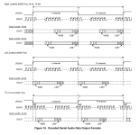
I2S data is in signed twos-compliment form, isn't it (at least for more than 8-bits of data?)?
OTOH it appears DACx1001 uses SPI bus and unsigned data?
Also, looks like timing and programming waveforms are shown on pages 15 and 27 of the datasheet: https://www.ti.com/lit/ds/symlink/dac81001.pdf?ts=1710698978453&ref_url=https%3A%2F%2Fwww.google.com%2F
DAC-DATA format is on page 30.
Also, when LRCK is high the the Left channel data is sent; LRCK low is the the Right channel. DACx1001 appears to be a mono dac, so you need two of them?
Seems like it would probably make sense to draw out the I2S input waveforms including their incoming justification from the source device (in one color or otherwise easy to distinguish from SPI), along with desired output SPI waveforms. From that it should be pretty clear which clock and data is which. Also, since DACx1001 appears to read data on the falling clock edge whereas I2S writes data on the rising edge, that should difference also be shown clearly.
Another consideration might be that I2S bus usually runs at 3.3v LVCMOS levels. What voltage will you be operating DACx1001 at?
IOW, the more you organize this the more likely it would be for other people to step in and help, and you might even find you know the answer already from doing the timing analysis.
Regarding sim at: https://www.falstad.com/circuit/cir...QN1NgElO6lx3Bk5jNjaDTrO8+z4RM3wzbczAsgywz4hAA

The LD pin appears to be used as a data input and the Serial Input pin is left floating?
https://www.ti.com/lit/an/scea117/s...31761&ref_url=https%3A%2F%2Fwww.google.com%2F
The LD pin appears to be used as a data input and the Serial Input pin is left floating?
https://www.ti.com/lit/an/scea117/s...31761&ref_url=https%3A%2F%2Fwww.google.com%2F
You need to read the post linked in OP for context.
Basically all the hard work was done by a TI rep who provided a glue logic circuit for the DACx1001 to convert a 24bit right justified input to SPI for two DACx1001s in the daisy-chain config
Then all Im trying to achieve is modifying the glue logic circuit to work with an i2s input instead of 24bit right justified input, which I may have managed already.
But regardless of the data input format, I can't understand how the glue logic works correctly from looking at the simulation.
Looks like @PaulFrost isnt active on the forum anymore.
Last edited:
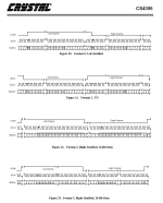
Page 27 of the datasheet looks like the data write is left justified whether daisy-chained or not. D23 is first and D0 is last in both cases. Also if you search the datasheet for the word, justified, it only turns up instances of left-justified. That said, some USB boards can probably send left-justified format (maybe I2SoverUSB). Even if so, there are still other considerations.
Moving along to the next thing, don't know what Paul Frost meant about daisy-chain being more like I2S. It looks like the only difference is if sync is enabled for more than 32-bits into Din then it ripples out through Dout.
Also besides DAC-DATA [D23-D0] in register 01h there may be other registers to configure/write, unless maybe you want all the reset defaults?
So, I think there is no way forward but to study the datasheet, decide how you want to operate the device, then write the appropriate bits according to the timing diagrams. It might take a few hours to figure out, but what you are doing now is taking how long?
Last edited:
The data is "left justified" at d23 in a 32bit register, a data input in the 24bit RJ audio format ends up "left justified" at d23 also.Page 27 of the datasheet looks like the data write is left justified whether daisy-chained or not. D23 is first and D0 is last in both cases. Also if you search the datasheet for the word, justified, it only turns up instances of left-justified. That said, some USB boards can probably send left-justified format (maybe I2SoverUSB). Even if so, there are still other considerations.
daisy-chain mode probably allows simpler glue logic.Moving along to the next thing, don't know what Paul Frost meant about daisy-chain being more like I2S. It looks like the only difference is if sync is enabled for more than 32-bits into Din then it ripples out through Dout.
I had not seen anything that needed to be changed from the default.Also besides DAC-DATA [D23-D0] in register 01h there may be other registers to configure/write, unless maybe you want all the reset defaults?
what am I doing now then?So, I think there is no way forward but to study the datasheet, decide how you want to operate the device, then write the appropriate bits according to the timing diagrams. It might take a few hours to figure out, but what you are doing now is taking how long?
Waiting for someone to give you the answers?...what am I doing now then?
I2S data is two's complement form. What glue logic will you use to fix that?
What you probably need in reality is something more like an FPGA. Work out the logic and program it to do the work. If the logic has errors, then troubleshoot with a scope and or logic analyzer until you figure out how to get the bit patterns you need.
What you probably need in reality is something more like an FPGA. Work out the logic and program it to do the work. If the logic has errors, then troubleshoot with a scope and or logic analyzer until you figure out how to get the bit patterns you need.
I see there has been some confusion, you already gave me the answer I was looking for earlier and I didnt realise, simply that is not is as simple as I thought... so thank you.Waiting for someone to give you the answers?
i2s data is signed and it seems the mentioned "24-bit, right-justified I2S" is or at least can be unsigned?
I thought they were the same so never bothered to look into the differences between signed and unsigned data.
Information on this scarce.
e.g From the DIR9001 datasheet, 24bit RJ and I2S outputs are both 2s-complement:
This diagram that seems to imply RJ is unsigned, since only I2S and LJ have negative bit numbers:
I2SoverUSB manual does not mention anything about two's complement, unsigned, signed etc.
Nor CS8412
Nor AK4137
?You can use any 32-bit RJ I2S input. For example, you can use a DIR and skip the MCU all together.
Attachments
Last edited:
For twos-compliment format, the MSB is the sign bit. If its 1 then the number is negative.
Also IIRC, 8-bit I2S may be unsigned (?). 16-bit and higher is signed.
In addition, a quote:
Data is signed, encoded as two's complement with the MSB (most significant bit) first.[1] This allows the number of bits per frame to be arbitrary, with no negotiation required between transmitter and receiver.[1]
https://en.wikipedia.org/wiki/I²S
Also a wiki for SPI bus:
https://en.wikipedia.org/wiki/Serial_Peripheral_Interface
The thing about datasheets is that they have an intended audience. Time was when there was a barrier to access and those who did have access, by and large, also had the prerequisite knowledge to make sense of them and certain things need not be said. The increased availability of said datasheets has not changed that. Information isn't scarce. It is simply assumed you know your stuff.
As it happens, the demo config code in the DACx1001 datasheet serves to confirm what the register listing states. The data is straight or unsigned binary.
As it happens, the demo config code in the DACx1001 datasheet serves to confirm what the register listing states. The data is straight or unsigned binary.
The DACx1001 can be configured for unipolar or bipolar output.
I think the DAC register supports data in two's complement for a bipolar output, despite how the datasheet words it.
Its the only way to explain how the glue logic would work.
Following this explanation, the behaviour of the sim can also be explained.
The MSB being inverted is the sign bit, not a data bit.
Last edited:
Unipolar or bipolar is only determined by the negative voltage reference. Either way, the DAC-DATA code only determines where in-between the two reference voltages the dac analog output will be.
So, if you want a pretty negative voltage in bipolar mode then the MSB would be have to be zero, wouldn't it? If so, then the MSB is not the sign bit of two's compliment.
Last edited:
So the possibilities we have:
- The DAC doesn't support 2s complement and the TI rep assigned to promote the DAC for audio use has missed a fundamental detail when designing the glue logic for it.
- There exists some uncommon RJ "I2S" format with unsigned data and I can no longer understand how the logic sim works since the MSB is being inverted.
- The DAC has support for 2s complement but the datasheet makes no indication of this.
What do you mean by negative? In unsigned binary there is only positive. Two's compliment allows for negative numbers.
A negative number in two's complement, if you take its bit pattern and interpret it as unsigned, then it would be a positive number at or above half-scale (because the MSB is set).
What the equation says is that there is a reference voltage span, in parenthesis, multiplied by a ratio from 0 to 1, plus the negative offset of the negative reference. So if the ratio is zero, you get the most negative possible value. To get zero the numerator has to be zero. To get the maximum positive output voltage the ratio must be 1. That means the numerator must be the the number of bits your particular dac has.
Last edited:
- Home
- Source & Line
- Digital Line Level
- TI DACx1001 discussion - I2S input, Vref etc