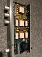
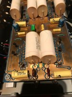
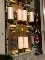
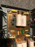
analog_sa said:Huh. My PCB is quite different - also a series II.
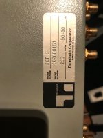
That is different! My S/N is 185060365. Is mine newer or older than yours?
Bill
Mine is clearly older - 184030014. Phono connections use much longer internal wires instead of pcb tracks. Funny thing is these wires and the outputs are silver in teflon and all other inputs use standard pvc copper. Mr Pass didn't like cd sound 20 years ago 🙂
Vol pot is Noble and may well be 25k - already put the lid back on.
Vol pot is Noble and may well be 25k - already put the lid back on.
MashBill and Analog_sa, thanks for posting the pictures. Nice🙂
Steen🙂
It does make a difference. When wiring the pot at the output you raise the output impedance of the preamp, throwing away some of your signal in the process. The pot is often wired at the output of a BoZ or BosoZ, but those preamps has enough output, so you can afford to throw some of it away. The advantage of wiring it at the output is, as you mentioned, that the circuit noise is attenuated when turning down the volume. Furthermore the pots at the output of the BoZ/BosoZ family is only 5-10K, which makes it a bit more acceptable. The "normal" thing is to wire the pot at the input of a preamp, though.Does it make a difference or just preference?
Steen🙂
All the parts are available at Mouser, except the 3N172. It's described as a P-Ch enhancement mode mosfet. Diagram shows 4 leads. Any substitutes?
The 2N5566 FETs are dual FETs. They are over $14 a piece.
The 2N5566 FETs are dual FETs. They are over $14 a piece.
vdi_nenna said:All the parts are available at Mouser, except the 3N172. It's described as a P-Ch enhancement mode mosfet. Diagram shows 4 leads. Any substitutes?
The 2N5566 FETs are dual FETs. They are over $14 a piece.
Earlier in the thread i mentioned easily available replacements - 2sk389 for the fets and zvp3310 for the mosfet. Both have been endorsed by Mr Pass in previous threads.
Btw, in post #1 i described the PS transformer as being 30VA. Wrong, it's just 15VA.
It's interesting to compare the phono section to an Aleph Ono. It's very similar with some of the CCS being replaced with cascodes and the complementary source follower at output more capable of driving long cables and the scaled down riaa network.
Looking at the circuits, the FET 2 may well sound more transparent. In practice my Ono clone sounds better (with the exception of the bass which is deeper but not as tuneful) but it's a really unfair comparison with all the top grade components in the Ono.
A FET 2, built with nice parts and good regulators, preferably separate for each stage, might sound really nice.
Earlier in the thread i mentioned easily available replacements - 2sk389 for the fets and zvp3310 for the mosfet. Both have been endorsed by Mr Pass in previous threads.
I reread, but missed the replacement parts, sorry. 😱
I think I'm going to try the line amp section.
I've been doing some simulation on a similar circuit using 2SJ74 and ZVP3306, with current mirror load and tail current generator slaved to a master current source/reference. The big difference is that I cascoded the input differential stage to get rid of the Miller capacitance, as I'm looking at using the circuit in an RIAA stage.
Due to the cascode and the increased gm of the new devices over the originals, I find the new circuit to be pretty slippery and requiring lag compensation on the output stage to prevent HF rail to rail oscillation. The P-channel lateral output MOSFET used in the original circuit undoubtedly had a much lower transconductance than the newer vertical relacement devices. Both the 2SJ74 and 2SK389 have at least twice the transconductance of the 2N5566. A pair of matched PN4393s would probably be a closer replacement for the 2N5566.
I'm going to continue messing around with the simulation until I get some results that suit me. One thing that I found out right away is that it is necessary to very closely match the current source load current to the expected device current in the differential stage in order to minimize distortion.
A possible replacemet candidate for the original output MOSFET might be one of the new FETs from Advanced Linear Devices (available from Mouser).
wrenchone said:
Both the 2SJ74 and 2SK389 have at least twice the transconductance of the 2N5566.
not quite. 2N5566 7.5-12.5mS 2sk389 8-20mS
I would assume transconductance on the high side for the 2SK389s unless one is deliberately using GR ranking and current starving them. I found some source degeneration helped to tame the oscillations somewhat, as the models I'm using for the 2SJ74 appear equivalent to approximately BL rankng.
wrenchone said:The big difference is that I cascoded the input differential stage to get rid of the Miller capacitance, as I'm looking at using the circuit in an RIAA stage.
One production version used IT505 cascoded matched JFETs.
😎
IT505 - I haven't seen a part number like that in ages. Intersil, wasn't it? I used J174s for the cascode FETs in my simulation, as I have both models and devices in hand.
BTW, I was interested in doing the simulation (though not necessarily the real thing right away) to check out the open loop gain and closed loop distortion available from such a simple amp. Doing a feedback-style RIAA preamp asks a lot from the circuit in question.
BTW, I was interested in doing the simulation (though not necessarily the real thing right away) to check out the open loop gain and closed loop distortion available from such a simple amp. Doing a feedback-style RIAA preamp asks a lot from the circuit in question.
Hi
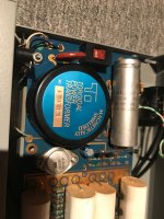
I was looking at the picture in post 16 and wondered if anyone could tell me what the grey box next to the transformer was ( I think it says Midland cross on it ). Is it a servo or a reed switch?
Don
I was looking at the picture in post 16 and wondered if anyone could tell me what the grey box next to the transformer was ( I think it says Midland cross on it ). Is it a servo or a reed switch?
Don
Any substitute?
Hello,
I'm wondering if it would be possible to use 2sk170 or 2sk30 instead of 2n5566?
Hello,
I'm wondering if it would be possible to use 2sk170 or 2sk30 instead of 2n5566?
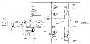
analog_sa said:The diode-looking thingies are, of course CCS; couldn't find a more convincing-looking symbol in Protel. J505 - 1mA, J507 - 1.8mA, J511 - 4.7mA.
There is a muting relay in parallel to the output. It has a 10s delay on power-on and a connection to the power switch to instantly mute at power-off.
Would anyone tell me where is the diode J507? I can not found it on any of the 3 circuits posted. There are only J505 & J511 diodes.
Thanks
HKC said:
Would anyone tell me where is the diode J507? I can not found it on any of the 3 circuits posted. There are only J505 & J511 diodes.
Thanks
Sorry should be J511. There are only J505 & J507 on the circuits no J511.
Threshold FET2 Series II - muted MC input one channel
Hi,
I'm new to this thread.
I noticed the earlier discussion and attached supporting schematics by another poster for a FET 2 Series I, thanks for sharing.
I have a FET 2 Series II (series 2) with one MC channel (left) muted (maybe by 30dB or more). I can hear sound when volume pot is turned way up, but noticeably lower than the right channel. The MM and line level inputs work fine for both the L&R channels. In other words, when I play a CD or tuner, or Phono with MM cartridge, both channels produce undistorted audio at similar power levels. It appears that just the one MC input and associated circuitry is affected by the noticeable attenuation. NOTE: I also verified that both the MC/MM external selector switch and input cap/res loading switch are working properly.
Question: Is the FET 2 Series II schematic different than the FET 2 Series I regarding the MC stage? Does someone have a FET 2 Series II schematic they can post (thank you)?
Going forward, assuming that the FET 2 series 1 and series 2 MC schematics are identical, here are my next debug steps and considerations (please advise if I'm overlooking something):
1) Verify the J50x series diodes (505, 507, & 510) are OK
2) Verify that the 2N5566 is OK (perhaps swap out with the working channel and verify?)
3) Verify that the 470uF electrolytic cap with neg lead connected to R8 and R2 is OK (assumes R8 and R2 are also populated on the series 2 version)
4) What else....can the silver mica caps go bad?
5) Any other suggestions on how to fix?
Thank you in advance for you help.
Reviving an old thread here 🙂
Seems like there's several versions of the FET TWO - mine looks very different!
Seems like there's several versions of the FET TWO - mine looks very different!
Attachments
-
 84812258_1085632275106869_3828483746860892160_n.jpg148.4 KB · Views: 227
 -
 89716230_254964925506575_1659961283165814784_n.jpg229.7 KB · Views: 229
 -
 89721949_2750464525030645_8747075037200121856_n.jpg145.5 KB · Views: 223
 -
 89728114_138019557587491_300162516854505472_n.jpg342.3 KB · Views: 205
 -
 89781705_496056827743897_5909821243485323264_n.jpg132.8 KB · Views: 165
 -
 89810337_652183988691270_7746732104049754112_n.jpg148.1 KB · Views: 161
 -
 89839454_1077481112615371_5846587376289185792_n.jpg175.7 KB · Views: 150
- Home
- Amplifiers
- Pass Labs
- Threshold FET 2