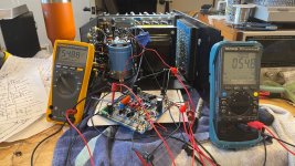
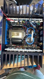
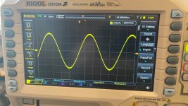
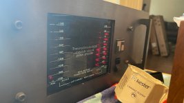
The screws go thru the heatsink. If any of these touches the heatsink, it will tie the TO-3 collector to it. I would verify every single one of these. Normal TO-3 mounting kits, such as the Aavid 4804G, include insulated shoulder washers.
All collectors checked , I measured no shorts to heatsink/gnd. Also checked B to E for each output. As well as C to E . No active shorts.
I disconnected the 1 ohm res. from output and measure dual diodes O.395V for each diode. Measured in opposite direction and it looked okay.
I was hoping to find something. If there were a shorting collector rail to ground there would be some serious current . On the dim bulb, it lights up during initial charge of main caps then comes back down. Which does not indicate a collector/rail short to ground.
Last edited:
Did you check with a DMM on resistance range that there are no shorts between each TO3 transistor case and the heatsink? Yes each mounting screw needs an insulating bush where they pass through the heatsink - these should all have been fitted on the original build.
The base and emitter for each component has thru hole guides. The screw to collector/nut on opposite side have guide holes. I don’t recall bushing on output board. But that being said no shorts from collector(s) to sink.
I did see bushings for screws on Varo 711xe dual diode.
Last edited:
Also measure the voltage over the cascode divider resistors. They will indicate whats going on.
The 1K ohm resister divider? This sets up the base voltage for the upper and lower Rail Quadrants?
Last edited:
I have +/- Rails bias at 55-56 V.
Board is grounded and thermal fuse is shorted
Diff pair has ~33mV delta on each side which is about 1mA per leg. Q10 delta across 330 ohm is then ~0.630V (2mA).
Q9 delta 0.62mV
Q19 (2n4250). delta 275mV.
Q7 base. = 2.35V
Q1 base = 2.2V
Delta across Q4 collector and Q2 collector (5k trim pot) is approximately 1.2-1.3V.
The resister divider on pos rail and neg rail ia approx half the rail at the midpoint. ~28V as rail is 56V.
Delta across res divider ~55-56V.
Last edited:
What bias do you have, and does offset change with bias?
I had outputs that worked with low bias, but above say 30 mA they did short. If it's the cascode you would see a voltage shift, and you can also measure if voltage rises over the output collectors. If it's an output you will see a current drop/rise over emitter resistors.
I had outputs that worked with low bias, but above say 30 mA they did short. If it's the cascode you would see a voltage shift, and you can also measure if voltage rises over the output collectors. If it's an output you will see a current drop/rise over emitter resistors.
What bias do you have, and does offset change with bias?
When i had the outputs connected to driver board bias was trimming into 65mV. DC offset was in the 30V range.
I could reconnect again. Set idle current to OmV and see if dc offset goes to OV or close to Ovolts.
Last edited:
The measurements i am showing on driver board appear that it is balanced? Would you concur? The drive stages i am not sure yet.
These are new outputs but i guess anything could happen. None appear shorted but are you suggesting they could be partially shorted?
These are new outputs but i guess anything could happen. None appear shorted but are you suggesting they could be partially shorted?
Yes driverboard voltages looks ok.
I had original transistors that measured ok with DMM and DCA-75, but in circuit they shorted when current rised. Like a switch with about 30 mA threshold.
You have to check if it's the cascode or the outputs. On one of the 2 4000's that I worked on I measured increased drop over the upper 1k cascode resistor indicating a large basecurrent, in 2 transistors that was shorted. There was also shorted outputs, and itt seems like if one or more outputs go, one or more cascodes give up.
It was some of those "Working" transistors that had the mentioned fault.
Well, all measures fine it seems statically on the OS and the driver board does not seem to show any problems as you have displayed the measurements not connected to the OS. The issue could be that one of the OS transistors is breaking down under current.
Slowly adjust from zero bias in steps while monitoring the DC output offset volts. If at some point the DC offset rises like before you should be able to measure across each output device/resistor to see where the DC voltage is being generated.
Slowly adjust from zero bias in steps while monitoring the DC output offset volts. If at some point the DC offset rises like before you should be able to measure across each output device/resistor to see where the DC voltage is being generated.
Slowly adjust from zero bias in steps while monitoring the DC output offset volts. If at some point the DC offset rises like before you should be able to measure across each output device/resistor to see where the DC voltage is being generated.
I’ll put it back together . I was going to remove two output stages from each quad. Then put it back together. Ill set bias to 0mV and ramp up while monitoring dc offset.
More to come!
I was thinking my part selection could be suspect msp42 and msp92 as the two driver stages. Im using a KSC733C for the 2N4250A.
But even so i wasn't expecting output to rail.
But even so i wasn't expecting output to rail.
You could measure transistors out of circuit with 10v PSU adjusting Vbe with a 10k pot,
I was able to get my hands on a tek 576. The DCA 75 are usually a decent home check with obvious limitations. But to be honest wasn’t expecting the half-railed output.
I bull dozed thru rebuilding the driver board. Bad!
It is a good idea to check the basics of the driver board prior to hooking it up to the output stages. Good!👍
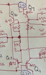
The drive stages with the heat dissipation TO-92 package. . What are you using on these models? Are you using TO-92 package or up the power dissipation i was thinking KSC2690 and KSA1220 for Q16/Q17. And MJE150xx for Q1/Q7.
This particular unit has two differently labeled versions of driver boards. CFE1078 on the Right and CFE379 on the left. At a glance their doesn’t appear much difference. Looking at boards i have not seen any prior edits.
Factory decision or a chopper?🤔 Possibly they ran out of 1078 boards and they put 0379 as next in line.
My drivers were ok so I never thought about swapping drivers. But I can think of 1381/3503, A1360/C3423 and alike with low Cob, or 1220/2690 or the new Toshiba drivers with a bit higher Cob. I don´t know if it changes the response, and I have no datasheet of the FT transistors.
The other amp I worked on was an older (one year) without those drivers, just MPSA42/92.
NP knows best I guess...
/Figge
The other amp I worked on was an older (one year) without those drivers, just MPSA42/92.
NP knows best I guess...
/Figge
I may give it a try and take some measurements. There are plenty of newer devices with like data sheets. The input diff pair standoff voltage cascode is not necessary if a high gain and higher Vce component is used. But i underStand why it’s in this schematic version with the lower voltage 6571’s.My drivers were ok so I never thought about swapping drivers. But I can think of 1381/3503, A1360/C3423 and alike with low Cob, or 1220/2690 or the new Toshiba drivers with a bit higher Cob. I
This might be a stupid comment/question, but do TO-3s require insulated shoulder washers to keep the screws from shorting the case (collector) to the heatsink?
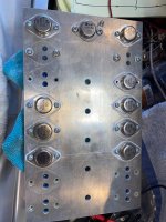
Fyi, confirmed each collector thru hole has a plastic tube insulator. All are in place. Pic below with removed pnp shows insulator. These do pop out if board is flipped . Definitely something to be mindful of if replacing outputs.
These insulators along with mica isolate collector from grounded sink.
Misc.
- Home
- Amplifiers
- Pass Labs
- Threshold 400A. L/R Channel out and fix
