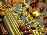
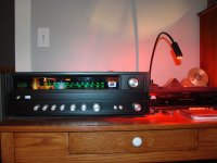
I`m working to fix a Threshold 400 amp for a friend.
So far we found one of the output transistors that was damaged
and a transistor and resistor on the circuit board that was also damaged.
The output transistor was replaced with the Onsemi 15024.
The transistor and resistor on the circuit board did not show outward signs of damage until the amp was up and running again after changing out the damaged output transistor.
If anyone knows which transistor and resistor we have that is damaged or can point us to a more accurate schematic it would be very helpful !
(The schematic on this site does not appear to exactly match our circuit board)
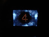
When the amp went out the LED display on the right side was max and the left side was at minimum. Once the output transistor was replaced the right side started working again, (left side still no output) and the LED display worked properly again.
(The damaged output transistor was on the left channel and we think it had taken out the transistor and resistor on the circuit board also when it blew).
The owner realized after the damage that the amp required 8ohm speakers but he had been running the amp on 4ohm speakers.
We believe this might have been the cause for the damage.
The amp had been running fine for about six months after being in storage for a year or so when the damage occured.
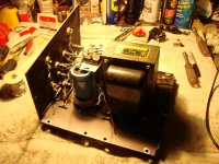
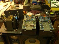
I have included a photo.
Thank you in advance, andrew
So far we found one of the output transistors that was damaged
and a transistor and resistor on the circuit board that was also damaged.
The output transistor was replaced with the Onsemi 15024.
The transistor and resistor on the circuit board did not show outward signs of damage until the amp was up and running again after changing out the damaged output transistor.
If anyone knows which transistor and resistor we have that is damaged or can point us to a more accurate schematic it would be very helpful !
(The schematic on this site does not appear to exactly match our circuit board)
When the amp went out the LED display on the right side was max and the left side was at minimum. Once the output transistor was replaced the right side started working again, (left side still no output) and the LED display worked properly again.
(The damaged output transistor was on the left channel and we think it had taken out the transistor and resistor on the circuit board also when it blew).
The owner realized after the damage that the amp required 8ohm speakers but he had been running the amp on 4ohm speakers.
We believe this might have been the cause for the damage.
The amp had been running fine for about six months after being in storage for a year or so when the damage occured.
I have included a photo.
Thank you in advance, andrew
Attachments

Last edited:

Did you search? I did a quick search and found a Threshold 400a parts subsitution & mods thread where I found this pdf.
By the way that amp will drive 4 ohm speakers all day long with no problem. Way back then this amp was popular they would even drive the
modified Dayton-Wright electrostatic speakers. The modified Dayton-Wright speaker was a verry verry bad load for an amp it was .5ohms above 5k. Thats right above 5k the modified Dayton-Wrights were about
1/2 ohm.
Attachments
Good morning woody !
Thanks for the response.
Yes we have done extensive searching for information.
The schematic you sent was one of the ones we have printed out
to help us along.
If you have a moment to take a close look you will see our dilemma.
There are 14 transistors shown on the circuit board portion of the schematic
yet we have 18 transistors on the board ?!?!?
I have spent hours following the circuit board traces from one component to another, from transistor to resistor to capacitor to identify which component occupies which designation, ie, T-8 or C-4 for example. We need to confirm the failed transistor so that we install the correct replacement.
We know we can just take the one from the other side and copy the characteristics to allow a replacement but we would like to know which one failed and identify its place in the overall scheme.
Some of them are obvious but when you get to the portion of the circuitry that gets near the additional transistors on the board the schematic diverges from what we actually have.
Reading through all the posts here it is obvious that there is some heavy duty brainpower here, we are hoping that someone will check in and point out where our approach is failing.
We are enjoying the experience of working our way down through the problem but its kinda like when you finally need to raise your hand and ask the teacher for a little guidance.
We recapped this machine about 6 months ago changing out only the caps that we could identify by value.
The amp ran like a bear for months until this breakdown.
Now that you have provided the information that the speaker load was probably not the cause of the breakdown our theory turns to the possibility that the old heat dissipation compound had melted out from under the output transistor which allowed it to fail. We can see where all of the original heat dissipation grease has melted and flowed out from under the components.
The running temperature of the amp appears to be right on the nose according the information we have so even though it runs hot it doesn`t appear to be outside of the recommended limits
Thoughts, comments ?
Thanks again for your response, the pieces of information that you provided helps us in our theorization.
andrew
Attachments
Hi P901 I'm new to DiyAudio and i have not worked on this amp but I have a schematic for the 400a.
Audiocure.
Audiocure.
Good morning Audiocure !
Thanks for the response.
Do you know if your schematic shows all 18 transistors on the board?
The schematic we have from this site is close but not exact, it only shows 14 transistors on the board.
Our copy of the schematic from this website also shows approximately 80%+ of resistors that do not match the circuit board we have.
This makes it difficult to "reverse" engineer to find our way to identification of the failed component without a doubt.
How would we go about getting your copy of the schematic?
Is it an original ?
Thanks again, andrew
Attachments
If all else fails ask Nelson. By the way I do seem to rember the amp didn't like cobra
speaker cables. These cables were built with ~ 50 pair of insulated 24 gage wire.
speaker cables. These cables were built with ~ 50 pair of insulated 24 gage wire.
If you use the old cobra cables or the Mogami wire of the same
era, an RC network 5 to 10 ohms in series with .1 uF across
the load takes care of any issues.
😎
era, an RC network 5 to 10 ohms in series with .1 uF across
the load takes care of any issues.
😎
Good morning Mr. Pass! ,
Thank you for the information on the speaker cables and the
schematic.
We are having a bit of a challenge in the fact that the schematic
shows a different component count on the circuit board than what we actually have.
(The schematic shows 14 transistors, our circuit board has 18).
We endevour to map the circuit board component by component to produce an "as built" drawing which we will then use to correlate the actual component against the type and value shown on the schematic and parts list.
Were there a number of variations of this amplifier ?
Thanks again ! andrew
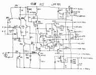
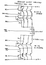
400a cascode schematics
Hi, P901 and Mr. Pass,
Hope this schematic, wich I made by "reverse engineering" of my own Cascoded 400a, is of interest for both.
Not exactly the same board as P901 have, mine is CFE379, but appear that the only difference is some resistors values.
The original schematics of cascoded 400a/4000 wich are circulating on the web, have an drawing error on output stage.
Regards,
Marcos
Attachments
Good morning Marco !
Thank you for that drawing !
We look forward to a detailed study later this evening !
I see you included a circuit board number CFE379, this means
to me that there were variants of this board ?
I will look more closely at our board, I presume the number is located
on the board ?
Do we know how many variants were produced ?
Thanks again ! andrew
Last edited:
Hi Andrew,
Yes, this is the number on the PCB. As yours, wich is CFE1078.
I think nobody knows the number of variations, except, maybe, Mr. Pass.
The major difference between variations, are input and LVA cascoded or not.
Your PCB is pretty the same as mine, except for little differences in some resistors. But, what is strange to me is a MPSA92 instead of 2N4250A.
Maybe the cause of explosion of the upper transistor of cascoded LVA (the heatsinked one) is a swap between MPSA92 and 2N4250A, the lower arm of cascode.
Regards,
Marcos
Attachments
Good afternoon Marco,
Thank you for the beautiful drawing !!
This is going to help us very much with our repair.
Would you please explain "LVA", I am not familiar with this term.
Also you say that there may have been a swap of transistors.
We have not changed any transistors and the amplifier ran for quite
a while but this is not to say that someone may have done some work
on this unit prior to our ownership.
Thank you again for the drawings, we are looking forward to getting the
drawings together with the circuit board tonight to hopefully determine exactly which component has failed and to research a proper replacement.
Regards, andrew
Attachments
Hi Andrew,
LVA stands for "Last voltage amplifier", in that case, a stage before triple darlington output. This stage, in cascode form, is made by transistors 2N4250A, MPSA92, 68r resistor, 20pf silvered mica and polarization components, two diodes, Res. 1K and Res. 15K.
About my suspicion, maybe your amp (1978, I guess) have originally two MPSA92 in this stage. My own amp, from 1979, and other schematics from Threshold I've seen, have 2N4250A in that position.
for your easy recognition, the abreviated word "DISSIP" marked next of four transistors in schematic, stands for "DISSIPADOR", our word for "Heatsink".
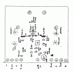
Output stage schematic attached. About the same Mr. Pass kindly give to us, except component values.
best regards,
Marcos
LVA stands for "Last voltage amplifier", in that case, a stage before triple darlington output. This stage, in cascode form, is made by transistors 2N4250A, MPSA92, 68r resistor, 20pf silvered mica and polarization components, two diodes, Res. 1K and Res. 15K.
About my suspicion, maybe your amp (1978, I guess) have originally two MPSA92 in this stage. My own amp, from 1979, and other schematics from Threshold I've seen, have 2N4250A in that position.
for your easy recognition, the abreviated word "DISSIP" marked next of four transistors in schematic, stands for "DISSIPADOR", our word for "Heatsink".
Output stage schematic attached. About the same Mr. Pass kindly give to us, except component values.
best regards,
Marcos
Attachments
Last edited:
I would guess CFE1078 identifies a pcb as created in October of 1978. If I'm correct, then CFE379 would have been created in March of 1979. I believe design enhancements were done on most pcbs, such that CFE1078 may have a few, several or most of the changes that would appear on CFE379. The schematics are dated, but don't necessarily correspond to each pcb design change.
There is a web site that has perhaps the finial version of the schematic and also a copy of the user manual.
Go to Threshold Lovers and become a register user. Once logged in, you will find a "Download" section you don't see as a visitor.
Under "Download" go to page 2, select "Threshold" then "Threshold T400A and T4000 diagram", then download "Threshold_400A-4000_diagram.zip". Once unzipped you will get "400a-4000_site.jpg", which is the schematic of 400A and 4000.
Similarly, on page 4, select "Threshold" then download "T400_user_manual_site.zip". Again, once unzipped you will find
"Site_Thresholdlover" (folder), which contains "Threshold_T400_user_manual" (folder), which then has individual pages - T400_p00_site.jpg
...
T400_p20_site.jpg
I know this seems indirect, but I am honoring Thresholdlovers request to NOT redistribute the file.
Good evening Marco !
It is very good of you to help us with this repair.
Your schematic has answered many questions.
It appears then that we have damaged the A92 Cascode LVA.
As a replacement we are looking at the MPSA92 High voltage amp.
It appears to have qualities above what would have been required
in the original configuration.
We also have the burned resistor 68 ohms to replace which appears to
be in this portion of the circuit.
Would you think it is reasonable to believe that a failure of one of the A8 output transistors could cause this collateral damage ?
We are hoping that the replacement of the damaged A8, the A92 and the 68 ohm resistor will put us back in operation.
Do you know if there is a "quick" way to test the section before applying power? For example would a resistance reading at some major point indicate whether or not we should begin to remove components from the board for individual examination.
Thank you again, andrew
Attachments
Good evening Mr. Brennan,
Thank you for providing the introduction to that site.
I have begun the process of registration and am awaiting
the confirmation response.
We are very much looking forward to viewing the new information !
Thank you again, andrew
Thank you for providing the introduction to that site.
I have begun the process of registration and am awaiting
the confirmation response.
We are very much looking forward to viewing the new information !
Thank you again, andrew
Hi Andrew,
I think is better to check all transistors and diodes on the board, but specially those with heatsinks and the other connected to 68r resistor, and, obviously, output transistors.
A series lamp on AC is a good measure of protection for the first time tests, and never connect anything at output, until you have checked DC operation.
Hope it help.
Marcos
Good morning Marco !
That sounds like good advice.
Interesting concept with a lamp on the AC in.
This will prevent damage of the components but allow
operation of the unit?
Any recommended wattage?
andrew
That sounds like good advice.
Interesting concept with a lamp on the AC in.
This will prevent damage of the components but allow
operation of the unit?
Any recommended wattage?
andrew
Ok, making progress,
Working along through the myriad of schematics that don`t actually
match the board we have.
Can anyone please give us some idea why there is a thermistor across
the Base/Emitter pins of the "first" power output transistor.
All the schematics we have show the thermistor going from the base pin
of the "first" transistor to the emitter of the "second" transistor with the emitter of the first transistor going to the base of the second transistor
so its not as if the connection shown on the schematic was physically achieved by an alternate execution.
What is the function of a temperature sensitive resistor across the B/E pins,
1.1K ohms cold, 300ohms hot.
Thank you, andrew
- Status
- Not open for further replies.
- Home
- Amplifiers
- Pass Labs
- Threshold 400 help