Good afternoon Mr. Pass !
Thank you for that feedback.
Not being an electronic engineer or designer it was
curious that the device was across the E/B pins on the one
transistor on the circuit board I have but in the three schematics it
was installed in another position across two transistors.
Was it found to be more effective or efficient in this position as
opposed to what is shown in the schematics?
Thanks again for the feedback, andrew
So, got a challenge here with the repair.
The right channel still works fine, the left channel failed.
Had three failed output transistors, two A92`s and one
2% tolerance 1K resistor had "drifted" to 4K!
Going through the components one by one we have been able to
get to the point where the unit no longer blows the fuse but it slowly
"cooks" the two A92`s, the LVA and the one next to it.
Prior to energizing the unit it was carefully checked, one side against the other for all values of the components, "in situ", for resistance, capacitance and diode function. The numbers all matched, (trying to avoid removing all of the left channel components).
Anybody have this happen? Any suggestions would be helpful.
Possibly the new MPSA92 transistors or the OnSemi MJ 15025/4`s are not a close enough match? Could the mismatch cause a need for readjustment of the bias resistance? How to do that without burning transistors if that is the case.
My next step is to go over all the components again one by one before trying one more time. If it cooks these transistors again then I guess I will be forced to remove all the components individually for testing.
The unit had been recapped about 6 months ago and had been working fine.
The right side still works perfectly.
Thank you in advance, andrew
Hi Andrew,
You have too much current running through LVA. I guess this is caused by defective constant current source who supply the LVA (the MPSA42 on the lower side of LVA, togheter with 2x 1n4148, 150R and 470R) When all is OK with front end, you have aprox. 4.6mA in the LVA (0,69V over the 150 ohms resistor).
When you change output transistors, always substitute all 3 pieces from the same parallel group, at least, and with components from the same batch. There is no need for tight match between them, thanks to a high value for the emmiter resistors (0,68R). But, Never mix togheter new MJ's with old 2N's in the same parallel group.
All the best,
Marcos
Good evening Marco !
Thank you so much for that information !
I had suspected that something was out of balance but never having
worked on such a unit with my level of experience I was at a loss.
I will follow your guidance, this must be the problem since everything else
has been thouroughly checked and re-checked.
I have read that the current across the .68ohm resistors should be set at
90ma across the resistor. Would there be any benefit to lower this value so slightly as to cool the amp just a little bit to assist in the life of the components ?
Thank you again ! andrew
Ok, making progress,
Can anyone please give us some idea why there is a thermistor across
the Base/Emitter pins of the "first" power output transistor.
All the schematics we have show the thermistor going from the base pin
of the "first" transistor to the emitter of the "second" transistor with the emitter of the first transistor going to the base of the second transistor
so its not as if the connection shown on the schematic was physically achieved by an alternate execution.
Thank you, andrew
The schematic made by m2003br in post #14 shows the thermistor connected like you are describing.
All of the schematics show two thermistors. Do you also have two, both connected across the base/emitter pins?
May I suggest that the 5K bias adjust resistor has been turned or become shorted. Either could result in excess output idling current, such that the output transistor will over heat. When the first output transistor goes south, then the other two are additionally stressed, finally resulting in the other two also going south.
Verify that the bias adjust resistor is set the same for both channels to start with. The position should be near center.
Verify that the bias adjust resistor is set the same for both channels to start with. The position should be near center.
On second thought, the 5K adjustable resistor may have become open, not shorted. Check for "cold" solder joint.
You can read a complete description of the bias circuit by reading Nelson Pass US Patent 3995228 - Active bias circuit for operating push-pull amplifiers in class A mode.
You can read a complete description of the bias circuit by reading Nelson Pass US Patent 3995228 - Active bias circuit for operating push-pull amplifiers in class A mode.
Good morning James,
Thank you for those great suggestions !
I will verify the action and connection of the 5K bias resistor.
During our ownership of this amplifier we have not moved the position
of the 5K bias but I have made very small pinpoint ink marks of the
position.
My thought was that if someone with experience could tell me of a a "conservative" starting point in the controls resistance
then I could slowly ramp up near the recommended current levels until the
amp came up to temperature and then follow the final setting procedure.
As you suggest, not knowing if this control had been previously adjusted
I thought that it would be good technical practice to reset/reverify
the setting.
Regarding the thermistors, there is only the one as shown on Marco`
schematic. There is another device wired into the circuit board and
"glued" to the output transistor base plate. It must be the thermal
overload which appears to open the line between the A92 LVA and
the A42. No other thermistors.
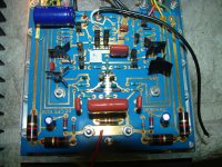
I have included a photo of the output section, you can see the two blue thermistors and the "overload" device glued to the plate.
(Also note that a couple of the resistors have been "lifted" while undergoing testing)
In the photo of the circuit board you will see the one transistor that I have marked with an orange dot. This was the other transistor that had partially failed along with the LVA A92. On the partially failed transistor once removed from the board I had from B to E .609 and from B to C .249 setting was on diode function with the Fluke 87V.
The failed devices have been replaced and you can also see the beige colored 68ohm resistor which is the one that had burned and split.
Awaiting a shipment of output transistors from Mouser and then we will begin again.
Thanks much to all for the help, andrew
Thank you for those great suggestions !
I will verify the action and connection of the 5K bias resistor.
During our ownership of this amplifier we have not moved the position
of the 5K bias but I have made very small pinpoint ink marks of the
position.
My thought was that if someone with experience could tell me of a a "conservative" starting point in the controls resistance
then I could slowly ramp up near the recommended current levels until the
amp came up to temperature and then follow the final setting procedure.
As you suggest, not knowing if this control had been previously adjusted
I thought that it would be good technical practice to reset/reverify
the setting.
Regarding the thermistors, there is only the one as shown on Marco`
schematic. There is another device wired into the circuit board and
"glued" to the output transistor base plate. It must be the thermal
overload which appears to open the line between the A92 LVA and
the A42. No other thermistors.
I have included a photo of the output section, you can see the two blue thermistors and the "overload" device glued to the plate.
(Also note that a couple of the resistors have been "lifted" while undergoing testing)
In the photo of the circuit board you will see the one transistor that I have marked with an orange dot. This was the other transistor that had partially failed along with the LVA A92. On the partially failed transistor once removed from the board I had from B to E .609 and from B to C .249 setting was on diode function with the Fluke 87V.
The failed devices have been replaced and you can also see the beige colored 68ohm resistor which is the one that had burned and split.
Awaiting a shipment of output transistors from Mouser and then we will begin again.
Thanks much to all for the help, andrew
Attachments
A bit of feedback,
Checked the 5K adjustable bias on both sides, Ok, good connection.
They were both set at 1.396K and had good function when
dialed up and down.
Would anyone know what an acceptable reading would be on the
"back to back" diode that it mounted in the center of the output plate
on one end? When removed from the plate each diode in the pack reads
.409 and a total of .811 through each other.
It says VARO R711XE on the case.
Good, bad ??
Thanks in advance, andrew
Hi Andrew,
The reading of the dual diode is OK. And, Don´t worry about trimpot adjustment.
Left it in a position for very little quiescent current, and make a final adjust after repair completed. with Higher resistance you get the lower current.
This is a good measure when use of a series lamp for tests. in this case, a 100 or 150W bulb is OK.
Marcos
VARO R711XE is Good.
Start bias adjustment at 0 ohms, which I believe will be full counterclockwise. At 0 ohms or even 1k ohms, you should have 0 current in the output stages, which you can determine by measuring the voltage across the 0.68 ohm emitter resistors on each of the NPN and PNP output transistors.
Start bias adjustment at 0 ohms, which I believe will be full counterclockwise. At 0 ohms or even 1k ohms, you should have 0 current in the output stages, which you can determine by measuring the voltage across the 0.68 ohm emitter resistors on each of the NPN and PNP output transistors.
Dear JamesBrennan,
I have to disagree with you. In the WONDERFUL 400A, for the sliding bias circuitry from Mr. Pass (and in all other good engineered amps, too!) you get the maximum current with the lowest resistance of trimpot. Because defective trimpots go to open state, and never to short circuit.
Regards,
Marcos
I have to disagree with you. In the WONDERFUL 400A, for the sliding bias circuitry from Mr. Pass (and in all other good engineered amps, too!) you get the maximum current with the lowest resistance of trimpot. Because defective trimpots go to open state, and never to short circuit.
Regards,
Marcos
Good morning gentlemen,
Thank you for that feedback, it goes a long way to helping
me understand the internal workings of this unit.
I will tell you that as I went further into my investigation I decided
to dismount the output transistors from the mounting plate.
I found one that had escaped my previous examination.
It appeared to have some value of function and I must have been
reading possibly parallel through the other mounted devices.
With this new piece of information I am hoping that this was the final
problem which was causing the odd slow failure of the other transistors.
We are currently awaiting a shipment of replacement output transistors.
As soon as the new components arrive and are installed we will post our
results.
Many thanks again for your help with this repair, andrew
Good morning all,
We had the opportunity to rebuild the output transistor section of the amplifier and with the help of the forum members we have success!
The amp runs with 245mv across the output transistors on the rebuilt side and 250mv on the original untouched side.
The temperatures are 119.2F on the rebuilt side and 121.1 on the original.
The manual gives us 90ma and 113F with the amp that utilizes the .068 resistors across the output transistors.
We will make the adjustments to the current values soon to hopefully get the current and temperature to the specified values.
Additional information.
Prior to operating the amplifier we decided to check the small value capacitors on the circuit board. (These had been left untouched since all previous schematics did not show the existence of and therefore the values.)
(These caps did not indicate a shorted condition or appearance of physical duress so during that period of time we decided to leave them alone) Once we had a good working schematic and due to the fact that our meter did not indicate any reading on these caps we decided to substitute the "closest" value we had on hand.
For the 390p we installed a 470n, for the 20p we installed an 18n, both polypropylene.
Yes, we have chastised ourselves for our impulsiveness for taking this direction after all of this work.
Fortunately the amp works and we ran for about two hours.
(We also revel in the amusement this must provide to the electronic engineers who truly understand the
consequences of this action. )
In this configuration though the L-R balance must be shifted to send 90% of the signal through this channel. The sound on this channel was very "boomy" with the mids being far in the background, almost an echo effect. Opposed against the original untouched channel it was quite an effect.
(Momentarily considered leaving it that way 🙂 )
The proper value replacements are due to arrive soon and we hope to have a fully functional unit.
Many thanks again to the forum members for their kind assistance, andrew
Last edited:
Hi Andrew,
Congratulations.
Guess you now know that a 20n is ~1000 times larger capacitance than a 18p.
I am curious, I didn't quite understand what you meant by
"I found one that had escaped my previous examination.
It appeared to have some value of function and I must have been
reading possibly parallel through the other mounted devices."
Was one of the output devices shorting to the heatsink?
James

Good morning Mr. Brennan,
🙂, yes a 1,000 times different.
We are hoping that this is the reason for the sound quality and signal level being "off".
Regarding the statement that I had found an additional output transistor which indicated a "value of conduction.
The initial approach to the overall repair was to disturb as little of the original amplifier as possible so therefore I did not summarily disassemble the major sections until indications would prove otherwise. When I believed that I had traced out all of the faulty output transistors I reassembled the unit and made numerous, resistance, capacitance and diode function "checkpoint" measurements throughout the unit. Being fortunate to have a mirror image fully functioning channel for side by side comparison and having the values match all along the way had the effect of raising the confidence level.
The only difference revealed was the point where the four small wires, (eight total, four for each side of the section) leave the circuit board and connect to the output transistor segment. The resistance reading was 4K between two of the wires, YtoGn if I recall correctly on both sides of the circuit board on the original untouched side of the amp and 3.8K on the rebuilt side.
With my level of experience I "convinced" myself that this must be the accumulated difference of the new OnSemi transistors as oppposed to the accumulated readings of the original Motorola` on the untouched side of the amp.
In this configuration the fuse was no longer blowing but the LVA transistor very slowly burned up. This then drove me to completely break down the output section and test each device individually. One transistor out of the complete package then revealed a reading of .243 on diode function of the meter from C to E if memory serves.
At this point the output section was completely rebuilt with a full set of the OnSemi MJ15025 and MJ15024.
A reassembly with another multi point side by side check now indicated 4Kohms and 4Kohms on both sides of each circuit board section and both sides of the amp. At this point the small caps were checked, (this is the point of the impulsive substitution since confidence and anticipation were running high).
The amplifier is now operating albeit with the "murky" sound which we hope will clear up once the proper small value caps are replaced.
Regards, andrew
Hi Andrew,
Congratulations for your success.
But, please, put back the original Silvered MICA caps. This is a (almost) "bullet-proof" component, never requires substitution.
My poorly hand-drafted schematic shows all three little caps, for sure.
Regards,
Marcos
Congratulations for your success.
But, please, put back the original Silvered MICA caps. This is a (almost) "bullet-proof" component, never requires substitution.
My poorly hand-drafted schematic shows all three little caps, for sure.
Regards,
Marcos
Good evening Marco !
Very nice to hear from you !
Yes, most certainly those Mica caps will be reinstalled.
Since this amp received some manner of duress to its system
we will be replacing the old mica caps with new ones per
your schematic.
I agree with you and from what I have read these are very
resilient components. Since I was not able to obtain a reading
with my meter I thought best to replace with new and these will
be of the indicated values on the schematic.
I will post soon when the final parts are in place.
We hope for a succesful conclusion !
Thank you again for all your help and I hope others who may experience the same difficulty will benefit from your knowledge.
Regards, andrew
Last edited:
- Status
- Not open for further replies.
- Home
- Amplifiers
- Pass Labs
- Threshold 400 help