ACK on both counts.I think Darlington/Sziklai is "two stages". It only looks like it is as easy as one part. The Sziklai in particular is likely to give more trouble than most 2-stage amps.
Only because the simulation doesn't check for it. Doing the math, we are at close to 0.9 W per transistor. That plus no emitter resistors is likely to mean that the thing would blow up in short order in real life - output stage first, VAS second.Even with '2222 it won't blow-up at idle.
Not to mention that you can always tell the designer's grey beard by the choice of non-E-series resistor values. 😉I'm not worried you will turn this in because it uses techniques older than your teacher and he/she will wonder where you got it from.
Still, it's a good illustration of the basic Lin topology. Not too far from a 4558 opamp.
As I've tried to explain to you in other threads in other places, the beta (Bf) listed in the LTSpice model is valid only under specific conditions. There are other paramenters in the model file that causes the beta to depart from the Bf value.
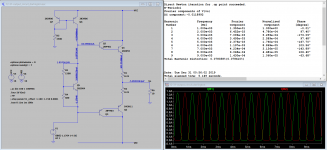
In that test .asc I posted to you elsewhere (reposted here), you can see that using the LTSpice built in model the 2N3055 is down to around 30 for a beta at a Ic=1.4 amps.
As an exercise, I created new models for both your output devices listing *only* the Bf values. With nothing in the model to modify these, the device will maintain a beta of 73 out to whatever current you want to pass. Distortion is greatly reduced.
Hope this all helps you understand what is happening.
Attachments
> at close to 0.9 W per transistor.
Modern '2222 may stand a whole Watt for half a class period. However the Spec does not require a real-world proof. And there ARE more-suitable parts available in LTS. And if one foolishly uses a too-small transistor the high parasitic resistance may delay your just reward (smoke).
> grey beard by the choice of non-E-series
That's just lazy typing.
There are several styles of values. 100 and 125 made sense to my mind and fingers. You advocate for parts in regular stock, OK. And then you find newbies who carefully trial/error a 109.76543 Ohm resistor as "perfect" (and any other falls-over).
Here, I started from a "high" current in the input stage. "4mA" is high. And the output stage peaking something over 1A. With just three stages of current gain I knew I had to stagger the currents to a split-difference to get the most out of each. Using two thumbs I figured 67mA in the middle stage, so around 227r for R5 R4 together. 120 and 100 came to my finger. I figure a plan should work with 20% parts; if it won't, you have to explain any "high" precision part to your Product Manager. Meanwhile the Purchasing Agent can round my 125 to 120, I don't care.
The idea of having Preferred Values as colored dots on the slide-rule makes a certain sense. But IMHO the Designer should KNOW these values by heart. And yes, I do sometimes pick resistor values on the slide-rule, though in this case "80" was easily figured as 2k and 25. (OK, that's 81, but you never get in trouble making speech/music 0.1dB louder.)
Designing an amplifier is a recursive operation . It doesn't matter whether you start from the head or the tail, you always progress in spiral form getting to the target in inverse exponential pace similar to a capacitor charging by a fix resistor. Your amp is required to have a feedback with 3 stages, the first thing to decide, which stage is going to carry the dominant pole . This stage will be of low frequency response, whereas the other one must have more than the NFB you will apply . With 80khz bandwidth and minimum NFB=2450/80 fixes your dominant pole. It also fixes your open loop maximum distortion .
Well, I was told to start from the output... I don't know what to say... I will remember your advice for the future.Why "start at last stage?" Did God design you head-first? What if He gave you a brain no body could support? Or so many feet that no brain could manage them? "Healthy" designs start with a "pencil sketch" showing an over-all unity of balance with just enough detail to be confident that it can be finished.
Thanks for the schematic. You really provided much food for thought but I will stick with a Darlington configuration because there's no way I can explain where that schematic comes from....I'm not worried you will turn this in because it uses techniques older than your teacher and he/she will wonder where you got it from.
Which simulation program do you use?
Thanks for your support. I think this Beta topic is now clearer.Hope this all helps you understand what is happening.
I have to remember to design the circuit looking at Beta graphs or the lowest beta value specified in the datasheet for a certain range of Ic.
For this reason I'd also suggest something a little beefier than 2N3904/3906 in the output stage, regardless of whether EF2 or Sziklai. Maybe 2N4401/4403, 2N5550/5401, 2N2219A/2905A.
....
Another potential downside of the Sziklai is that it is basically impossible to transition 100% cleanly from "push" to "pull", there's always a bit of a glitch that needs to be kept at bay via feedback. They make a great Class A output stage though.
Thanks for the advice.
I've decided to use the Darlington configuration.
I've adopted 2N4401/4403 BJT as suggested.
100mA quiescent current is ok or is it too much?
There is very low distortion right now.
I have Rin=19.2kohm which is good (with the simple circuit was less than 400ohm which is bad I think).
I still have to fully understand how the preferred values you were talking about works so some values aren't still standard.
I haven't found a real formula, now that I have a Darlington configuration, to choose the voltage across Vbe multiplier. That value determines the quiescent current, right? I started from 2V and I changed resistors values in order to obtain the desired Icq... Maybe there is the formula Vbb=Vt*ln(Ic/Is) that I have used with the simple output stage that I have posted some posts ago, but using the Darlington config I got confused...
Attachments
Hi all
I've lowered the quiescent current a little bit, I've used some preferred values for the resistors and I've added a CE stage...
I can't understand why I cannot have the full +-14V swing at the output now...
Have I done something wrong? How can I improve the situation?
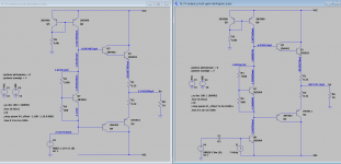
I attach the last stage schematic where I can have the full swing at the output and the output stage + CE stage where I cannot have the full swing.
I've lowered the quiescent current a little bit, I've used some preferred values for the resistors and I've added a CE stage...
I can't understand why I cannot have the full +-14V swing at the output now...
Have I done something wrong? How can I improve the situation?
I attach the last stage schematic where I can have the full swing at the output and the output stage + CE stage where I cannot have the full swing.
Attachments
The best and most simple way to understand the detailed operation of negative feedback is to analyze the Sziklai pair. I highly recommend this very easy and basic exercise to any student at an electronics college. He will have no choice but to find out that it uses voltage feedback just as it is in any feedback amplifier, current feedback operational amplifiers included despite their name.Essentially, a Sziklai pair (with a current sink or load resistor) is the most basic form of a current feedback operational amplifier, wired for unity gain. 40 years ago, people were regularly making up to line level gain stages based on this topology. They're pretty OK if you need 10-20 dB of gain.
Needs to be specified: What damping factor? DF= very low= current ampHi all
I'm designing my first 3 stages voltage amplifier as an electronics college course project.
Only BJT transistors present in LTSpice list are allowed.
Differential pair + common emitter stage + output stage.
Negative feedback.
As simple as possible. It is a simulation not followed by the real world implementation of it.
+-16V power supply
+- 175mV input signal swing corresponding to +- 14V output swing. (closed loop voltage gain = 80).
open loop gain of the 3 stages ampli = 2450 at least
resistive load >= 10ohm
amplifier input resistence >= 10kohm
bandwidth >=80 kHz
phase margin 80°
efficiency >=60%
THD <=1%
I've started from the last stage.
I've chosen Sziklai configuration (I hope it's not an overkill for this project).
I thought that after it was completed I could progress with the CE stage...
Unfortunately I've done something wrong and I've lost the biasing. I don't know how to progress... I thought that giving Q2 Ib= Ic/beta (read in the LTSpice model specifatios) would give me the conditions prior to the CE insertion but I was wrong... What do I have to do? Can someone please help me?
Distortion: at what frequency/power ?
Bandwidth: In amplifier world it means power bandwidth , or your teacher understands as frequency response.
It is required in the first place to be as simple as possible, Darlington choice is it as simple as possible?.
It wasn't specified.Needs to be specified: What damping factor? DF= very low= current amp
Distortion: at what frequency/power ?
Bandwidth: In amplifier world it means power bandwidth , or your teacher understands as frequency response.
It is required in the first place to be as simple as possible, Darlington choice is it as simple as possible?.
I thought the Darlington config was the simplest one to achieve the goal.
With +/-16v supply, when it output +/-14 v , the output transistors in Darlington must perform low distortion with 0.8v collector-emitter voltage at 1.4A ! I am not including yet the driver minimum voltage.
Adopting a Sziklai congig I could obtain the full +-14V swing.
I don't understand if that's due to something wrong I did with the Darlington version of the circuit or it's due to the fact that Sziklai have half tension across Vbe multiplier.
Happy new year
I don't understand if that's due to something wrong I did with the Darlington version of the circuit or it's due to the fact that Sziklai have half tension across Vbe multiplier.
Happy new year
Attachments
Sorry I am wrong with Vce , Fiesta effect. On the other hand this is not a real project but just a game to win on LT software. You can perfectly use current mirrors without degenerating resistors , you can also use the transistors to very low Vce as they aren't modeled the reality. You can replace the voltage multiplier by a resistor as no thermal variations are assigned. You can get rid of emitter resistors as the outputs function on an infinite heat sink, so no thermal runaway.
> I was told to start from the output...
As said: kokoriantz: "Designing an amplifier is a recursive operation . It doesn't matter whether you start from the head or the tail, you always progress in spiral form...."
Starting at the end *quickly* is a good first thought. Outputs are often harder than inputs. But inputs don't fall into laps either.
You may infer that "pole" was about my last concern. I wanted to get the DC conditions good, and see good output swing (overlooking the melting transistors).
> Which simulation program do you use?
My brain. I used to need pencil, paper, sometimes a slide-rule (they are incredibly handy).
For *posting*, drawing in Pspice is easier and clearer than scanning my scribbles. And it will do stuff I am too lazy to do for fun, like deriving the input bootstrapping (I had to change that three times because I was too lazy to actually look for the bottleneck).
And yes Pspice plot did show what my mind had suspected: three stages of same part at similar current WILL peak-up bad. Fortunately these too-small transistors are pretty speedy so a simple cap dominate the loop well above the audio band.
Last edited:
What does bootstrapping mean?>
For *posting*, drawing in Pspice is easier and clearer than scanning my scribbles. And it will do stuff I am too lazy to do for fun, like deriving the input bootstrapping (I had to change that three times because I was too lazy to actually look for the bottleneck).
Hi all
I've lowered the quiescent current a little bit, I've used some preferred values for the resistors and I've added a CE stage...
I can't understand why I cannot have the full +-14V swing at the output now...
Have I done something wrong? How can I improve the situation?
I attach the last stage schematic where I can have the full swing at the output and the output stage + CE stage where I cannot have the full swing.
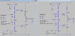
You reduced both the output and current source quiescent current when you increased R5 from 3500 to 6800 ohms and so reduced the available current drive to the pre drivers . Restore R5 to 3500 or 3300 ohms and reduce R3 to achieve the required output quiescent current . This should restore the max output voltage although with a Darlington output stage it is going to be close as it takes away another VBE voltage drop of available output voltage .
Hi all
When you project an amplifier like this one, what's the order of actions you follow? Do you project one stage after the other fixing the behaviour of each one before proceding with the next one?
I arrived at the input stage starting from the output stage.
It looks like I can obtain +-14V output voltage sweep. Good.
I have tried to adopt formulas used in class with ideal bjt (constant parameters) in order to find out the collector resistor value of the input stage but I got a negative resistor. I tried to consider the maximum voltage sweep that the input stage has to guarantee to the gain stage. I obtained this value dividing the voltage sweep at the input of the output stage (+-15V) by the voltage gain of the gain stage. Then I applied kirchhoff's node law.
Dropbox - formula dubt.docx - Simplify your life
I even asked in another forum about this problem: I was told to adopt 1mA in the input stage branches...
I did it but I still haven't understood why the method seen in class doesn't work in this case.
Dont' I have to consider voltage sweep in my computations? It looks to me that the method of considering 1mA is focused on quiescent voltages and currents. Am I wrong?
Cheers
Attachments
Last edited:
The output of the input stage is a current, not a voltage, in other words the input stage is transconductance amp (voltage in, current out), the VAS is transimpedance (current in, voltage out). At all but the lowest frequencies the transimpedance of the VAS is determined by the Miller compensation capacitor, not the transistors, since it sets up local feedback around the VAS transistor(s).
The transimpedance of the VAS at DC is affected mainly by its loading, which is why its typically given a constant current source load (very high impedance).
-----------
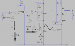
It illuminating to look at some typical voltage and current levels in the various stages:
The input might be 1Vrms with 50k load - thats 20uW at 50k ohms.
The signal fed to the VAS at HF, 7mV rms and 1mA rms, ie 7uW at 7 ohms (less power than the input, power loss factor 3 (-10dB), voltage loss 140, current gain 50)
The signal from the VAS to the OS: 30V rms, 1mA rms, ie 30mW at 30k ohms (power gain 4000 (+72dB), voltage gain 4000, current gain 1)
The signal from OS to speaker: 30V rms, 4A rms, 120W at 8 ohms (power gain 4000 (+72dB), voltage gain 1, current gain 4000)
Thus the VAS does an extraordinary job for a single transistor. The input stage's job is mainly to be differential, not to amplify.
The transimpedance of the VAS at DC is affected mainly by its loading, which is why its typically given a constant current source load (very high impedance).
-----------
It illuminating to look at some typical voltage and current levels in the various stages:
The input might be 1Vrms with 50k load - thats 20uW at 50k ohms.
The signal fed to the VAS at HF, 7mV rms and 1mA rms, ie 7uW at 7 ohms (less power than the input, power loss factor 3 (-10dB), voltage loss 140, current gain 50)
The signal from the VAS to the OS: 30V rms, 1mA rms, ie 30mW at 30k ohms (power gain 4000 (+72dB), voltage gain 4000, current gain 1)
The signal from OS to speaker: 30V rms, 4A rms, 120W at 8 ohms (power gain 4000 (+72dB), voltage gain 1, current gain 4000)
Thus the VAS does an extraordinary job for a single transistor. The input stage's job is mainly to be differential, not to amplify.
Last edited:
- Home
- Amplifiers
- Solid State
- Three stages amplifier college project help