Hi all
I'm designing my first 3 stages voltage amplifier as an electronics college course project.
Only BJT transistors present in LTSpice list are allowed.
Differential pair + common emitter stage + output stage.
Negative feedback.
As simple as possible. It is a simulation not followed by the real world implementation of it.
+-16V power supply
+- 175mV input signal swing corresponding to +- 14V output swing. (closed loop voltage gain = 80).
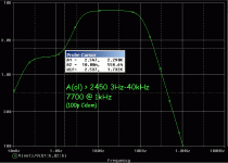
open loop gain of the 3 stages ampli = 2450 at least
resistive load >= 10ohm
amplifier input resistence >= 10kohm
bandwidth >=80 kHz
phase margin 80°
efficiency >=60%
THD <=1%
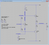
I've started from the last stage.
I've chosen Sziklai configuration (I hope it's not an overkill for this project).
I thought that after it was completed I could progress with the CE stage...
Unfortunately I've done something wrong and I've lost the biasing. I don't know how to progress... I thought that giving Q2 Ib= Ic/beta (read in the LTSpice model specifatios) would give me the conditions prior to the CE insertion but I was wrong... What do I have to do? Can someone please help me?
I'm designing my first 3 stages voltage amplifier as an electronics college course project.
Only BJT transistors present in LTSpice list are allowed.
Differential pair + common emitter stage + output stage.
Negative feedback.
As simple as possible. It is a simulation not followed by the real world implementation of it.
+-16V power supply
+- 175mV input signal swing corresponding to +- 14V output swing. (closed loop voltage gain = 80).
open loop gain of the 3 stages ampli = 2450 at least
resistive load >= 10ohm
amplifier input resistence >= 10kohm
bandwidth >=80 kHz
phase margin 80°
efficiency >=60%
THD <=1%
I've started from the last stage.
I've chosen Sziklai configuration (I hope it's not an overkill for this project).
I thought that after it was completed I could progress with the CE stage...
Unfortunately I've done something wrong and I've lost the biasing. I don't know how to progress... I thought that giving Q2 Ib= Ic/beta (read in the LTSpice model specifatios) would give me the conditions prior to the CE insertion but I was wrong... What do I have to do? Can someone please help me?
Attachments
With specifications like this
± 16 V power supply
± 175 mV input signal swing corresponding to ± 14 V output swing. (closed loop voltage gain = 80).
open loop gain of the 3 stages ampli = 2450+
resistive load > 10 Ω
amplifier input resistence > 10 kΩ
bandwidth > 80 kHz
phase margin 80°
efficiency > 60%
THD < 1%You're going to have a hard time accomplishing ALL those, along with '3 stages, and as simple as possible'.
Having a ± 16 V supply implies a 3 terminal supply … –16 V, 0=GND, +16 V; Biasing is usually pretty straight forward. I don't have a way to convert the .ASC file(s) to a graphic representation. Do us a favor, and take a screen-capture of a near-full-screen representation of the circuit, and post it. JPG is fine.
Just asking,
-= GoatGuy ✓ =-
± 16 V power supply
± 175 mV input signal swing corresponding to ± 14 V output swing. (closed loop voltage gain = 80).
open loop gain of the 3 stages ampli = 2450+
resistive load > 10 Ω
amplifier input resistence > 10 kΩ
bandwidth > 80 kHz
phase margin 80°
efficiency > 60%
THD < 1%
Having a ± 16 V supply implies a 3 terminal supply … –16 V, 0=GND, +16 V; Biasing is usually pretty straight forward. I don't have a way to convert the .ASC file(s) to a graphic representation. Do us a favor, and take a screen-capture of a near-full-screen representation of the circuit, and post it. JPG is fine.
Just asking,
-= GoatGuy ✓ =-
I thought that giving Q2 Ib= Ic/beta (read in the LTSpice model specifatios) would give me the conditions prior to the CE insertion but I was wrong... What do I have to do? Can someone please help me?
Don't think it is -quite- that simple. Parameter 'BF' in the model is defined only under very specific conditions, there are other parameters in the model that can cause the exact value of 'forward beta' to change. Try setting I1 to 25.6144 uA.
Having a ± 16 V supply implies a 3 terminal supply … –16 V, 0=GND, +16 V; Biasing is usually pretty straight forward. I don't have a way to convert the .ASC file(s) to a graphic representation. Do us a favor, and take a screen-capture of a near-full-screen representation of the circuit, and post it. JPG is fine.
Just asking,
-= GoatGuy ✓ =-
I think something pretty simple can be done because what has been taught during the course wasn't advanced at all... At least that's the hope...
Attachments

I'm speachless...Don't think it is -quite- that simple. Parameter 'BF' in the model is defined only under very specific conditions, there are other parameters in the model that can cause the exact value of 'forward beta' to change. Try setting I1 to 25.6144 uA.

Can you please tell me what are the steps I should follow to find that value?
There has to be some relations between quantities that I should use.
...I've lost the biasing. I don't know how to progress... I thought that giving Q2 Ib= Ic/beta ...
You are paying the school to teach you this stuff. Why do you have to go in dark alleys and talk to strangers to do your assignment??
WHAT "bias"? Voltage? Current?
I see you have TOO many digits on your current annotation; that just confuses quick reading.
You do NOT have current on the power devices. This will be important!
However I think your "bias" is that the output sat near-Zero VOLTage with a DC voltage source driving it, but with a *current* source (Ic/beta) the collector and center point will wander to ANY voltage.
Since you know you are required to have NFB when done, you should pencil-up enough of the design to have _DC_ NFB now. Compare the output to zero DC and force Q2 to force output to zero DC. Since Q2's input is nowhere near zero you probably want another stage, often called an Input stage, the assignment's Differential Input.
Last edited:
Maybe. He seems to be from the francophone world.You are paying the school to teach you this stuff.
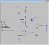
Anyway, common emitter stage Q4 is a transimpedance amplifier (current in, voltage out). We usually don't explicitly bias these, but rather give them an emitter current (as already present here) and then use their B-E drop to bias other stages.
It is fairly easy to turn this into something that even stands a decent chance of working in real life (the pesky thermal design possibly excepted, buncha TO-92s would not be making that too easy). I have taken the liberty to complete the circuit with a singleton input (giving an amplifier much like you might have found in a mid-'70s all-in-one stereo console). An LTP actually would make things even more straightforward, as you could eliminate the explicit input biasing and input AC coupling.
Homework for OP: Become intimately familiar with the E series up to at least E12, preferably E24.
Also, estimate AC open-loop gain at 100 Hz. (LTP input can also be done at DC.)
Can you come up with a simpler output stage that still meets the requirements?
Attachments
Last edited:
Just as a historical aside, regarding the E–6 (±20%), E–12 (±10%), and E–24 (±5%) scales…
Once, when engineering was denied any kind of digital computing resources (like, before 1960!), and when slide rules … ruled … the computational world, and engineering schools had to come up with useful pragma to teach their students and future practitioners, it was recognized that except for the rarest occasions, specific values for all kinds of components were on a POWER spectrum, rather than linear scale.
As a for-instance, one might get a 'nail' which was 2 mm diameter. The next useful one would be 2.5 mm. And another at about 3 mm. But when bridge-bolts were 20 mm diameter, there was absolutely no engineering reason to specify bolts at 21 mm.
2.5 ÷ 2.0 → 1.25 … = +25% 'more' diameter (squared = 1.25² = 1.56 or +56% strength ... for nails).
21 ÷ 20 → 1.05 … = ⊕5% more diameter (1.05² = 1.10 … or +10% ... strength for bolts, is this useful?).
So, for nails, screws, resistors, capacitors, inductors, and all nature of engineering 'things', the POWER scale because the most-rationally-used scale. It also was slide-rule friendly.
Technically, for an E–12 scale, each member should be 10¹⁄₁₂ = 1.2115277 times 'more' than the previous value. (that - 1) × 100 = 21.15%. Which is close enough to 20% that it was chosen as the international multiplicative value.
My Pickett “electrical engineering” slide rule actually had colored 'dots' at the E–6, E–12 and E–24 'standard values'. You'd compute away, and then when the answer would 'slide out', you'd just choose the nearest color-dot value. Life was easy. EASIER THAN CALCULATORS, for sure! … didn't require power, didn't die when dropped, useful as a ruler in a pinch (my Pickett had both inch, millimeter and some obscure French scale!). It also had 'dots' for all kinds of useful engineering constants. Brightness sequence of stars, you name it.
But nevermind slide rules.
E–6 … ±20% (+46.8% between values) are
E–12 … ±10% (21.2% between values) are
E–24 … ± 5% (10.1% between values) are
… where bold is “from previous sequence” …
And so on. The Wikipedia article on this is actually quite good, tho' a bit involved.
E series of preferred numbers - Wikipedia
Just reminiscing.
-= GoatGuy ✓ =-
Once, when engineering was denied any kind of digital computing resources (like, before 1960!), and when slide rules … ruled … the computational world, and engineering schools had to come up with useful pragma to teach their students and future practitioners, it was recognized that except for the rarest occasions, specific values for all kinds of components were on a POWER spectrum, rather than linear scale.
As a for-instance, one might get a 'nail' which was 2 mm diameter. The next useful one would be 2.5 mm. And another at about 3 mm. But when bridge-bolts were 20 mm diameter, there was absolutely no engineering reason to specify bolts at 21 mm.
2.5 ÷ 2.0 → 1.25 … = +25% 'more' diameter (squared = 1.25² = 1.56 or +56% strength ... for nails).
21 ÷ 20 → 1.05 … = ⊕5% more diameter (1.05² = 1.10 … or +10% ... strength for bolts, is this useful?).
So, for nails, screws, resistors, capacitors, inductors, and all nature of engineering 'things', the POWER scale because the most-rationally-used scale. It also was slide-rule friendly.
Technically, for an E–12 scale, each member should be 10¹⁄₁₂ = 1.2115277 times 'more' than the previous value. (that - 1) × 100 = 21.15%. Which is close enough to 20% that it was chosen as the international multiplicative value.
My Pickett “electrical engineering” slide rule actually had colored 'dots' at the E–6, E–12 and E–24 'standard values'. You'd compute away, and then when the answer would 'slide out', you'd just choose the nearest color-dot value. Life was easy. EASIER THAN CALCULATORS, for sure! … didn't require power, didn't die when dropped, useful as a ruler in a pinch (my Pickett had both inch, millimeter and some obscure French scale!). It also had 'dots' for all kinds of useful engineering constants. Brightness sequence of stars, you name it.
But nevermind slide rules.
E–6 … ±20% (+46.8% between values) are
E–6 = {10, 15, 22, 33, 47, 68}
… 100, 150, … 680 … and so on.E–12 … ±10% (21.2% between values) are
E–12 = {10, 12, 15, 18, 22, 27, 33, 39, 47, 56, 68, 82}
for the 10-to–100 decade. E–24 … ± 5% (10.1% between values) are
E–24 = {10, 11, 12, 13, 15, 16, 18, 20, 22, 24, 27, 30, 33, 36, 39, 43, 47, 51, 56, 62, 68, 75, 82, 91}
… where bold is “from previous sequence” …
And so on. The Wikipedia article on this is actually quite good, tho' a bit involved.
E series of preferred numbers - Wikipedia
Just reminiscing.
-= GoatGuy ✓ =-
Last edited:
Thanks a lot for the advice.It is fairly easy to turn this into something that even stands a decent chance of working in real life (the pesky thermal design possibly excepted, buncha TO-92s would not be making that too easy). I have taken the liberty to complete the circuit with a singleton input (giving an amplifier much like you might have found in a mid-'70s all-in-one stereo console). An LTP actually would make things even more straightforward, as you could eliminate the explicit input biasing and input AC coupling.
I would prefere a BJT differential pair as input stage (as I've seen during the course). In the next hours I'll try to sort it out.
How have you chosen the speed-up resistors values? Do I need them in my project?
I still don't know. Do you think it's possible?Can you come up with a simpler output stage that still meets the requirements?
Hi all
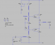
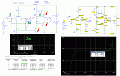
Out of curiosity I tried a simpler output stage.
I thought I biased it correctly. Am I wrong?
There is a lot of distortion.... A lot...
Since I have to use those two output transistor do you think I can improve this circuit behaviour?
Why the Sziklai version performs better?
Cheers
Out of curiosity I tried a simpler output stage.
I thought I biased it correctly. Am I wrong?
There is a lot of distortion.... A lot...
Since I have to use those two output transistor do you think I can improve this circuit behaviour?
Why the Sziklai version performs better?
Cheers
Attachments
Files attached for comparison.Hi all
Why the Sziklai version performs better?
Cheers
Attachments
Because the Darlington / Sziklai requires only about a 4 mA drive to deliver 1,200 mA to the load at near VCC and VEE. The “naked” transistors require at least 30 mA to 'get there', with both IBASE and ICOL summed.
You've only got a 25 mA current source 'up there'; as well, the 25 mA is shared between both the bottom output transistor and the top one. So…
Anyway, you could 'fix' this just by scaling the current-source to 75 or 100 mA.
At least that's my bet.
Just Saying,
-= GoatGuy ✓ =-
You've only got a 25 mA current source 'up there'; as well, the 25 mA is shared between both the bottom output transistor and the top one. So…
Anyway, you could 'fix' this just by scaling the current-source to 75 or 100 mA.
At least that's my bet.
Just Saying,
-= GoatGuy ✓ =-
Thanks for the kind reply.Because the Darlington / Sziklai requires only about a 4 mA drive to deliver 1,200 mA to the load at near VCC and VEE. The “naked” transistors require at least 30 mA to 'get there', with both IBASE and ICOL summed.
You've only got a 25 mA current source 'up there'; as well, the 25 mA is shared between both the bottom output transistor and the top one. So…
Anyway, you could 'fix' this just by scaling the current-source to 75 or 100 mA.
At least that's my bet.
Just Saying,
-= GoatGuy ✓ =-
I thought that the current source just needed to be greater than the maximum Ib at Ie_peak=1.4A
The gain of that transistor is 66 (from LTSpice parameters) so I did Ie_peak/66=Ib_peak=21mA
I left 4mA for the Vbe multiplier and I thought I was ok
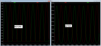
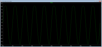
Rising current source value to 75mA improves the distortion a lot!
I don't understand how I can choose that value. Just trying to increasing it and looking at the result?
Cheers
Last edited:
The 2N3055 has very low gain, and gain that falls precipitously with increasing current, which is why its been obsolete for decades.
There's a reason why you'd generally see at least a two-stage emitter follower in speaker amps, with the outputs being preceded by another stage using medium power transistors (idling at ~6 mA, typ).
BTW, sizing for best-case beta is generally a bad idea. You need to study the beta over Ic graphs in the datasheet, at which point you will discover that every transistor has varying amounts of what's called "beta droop" at high currents, old ones like the 2N3055 quite a lot even.
For this reason I'd also suggest something a little beefier than 2N3904/3906 in the output stage, regardless of whether EF2 or Sziklai. Maybe 2N4401/4403, 2N5550/5401, 2N2219A/2905A.
Essentially, a Sziklai pair (with a current sink or load resistor) is the most basic form of a current feedback operational amplifier, wired for unity gain. 40 years ago, people were regularly making up to line level gain stages based on this topology. They're pretty OK if you need 10-20 dB of gain.
Sizing what you call the speedup resistor on the Sziklai is a matter of how much current the first transistor needs to operate well, depending on its beta(Ic) and fT(Ic) characteristics and power dissipation constraints.
You have to be a bit careful with this to maintain dominant pole compensation under all operation conditions, or else the output stage may break into local oscillation. The lower half pnp driver in a Sziklai push-pull famously tends to appreciate some Miller capacitance.
Another potential downside of the Sziklai is that it is basically impossible to transition 100% cleanly from "push" to "pull", there's always a bit of a glitch that needs to be kept at bay via feedback. They make a great Class A output stage though.
Generally speaking, you always have a tradeoff between circuit complexity, power usage and performance, with individual device performance playing a role as well. This is something to remember.
BTW, sizing for best-case beta is generally a bad idea. You need to study the beta over Ic graphs in the datasheet, at which point you will discover that every transistor has varying amounts of what's called "beta droop" at high currents, old ones like the 2N3055 quite a lot even.
For this reason I'd also suggest something a little beefier than 2N3904/3906 in the output stage, regardless of whether EF2 or Sziklai. Maybe 2N4401/4403, 2N5550/5401, 2N2219A/2905A.
The Sziklai uses plenty of extra negative feedback, thanks to its second transistor. This gives it a much higher input impedance and hence, lower input current demands.Why the Sziklai version performs better?
Essentially, a Sziklai pair (with a current sink or load resistor) is the most basic form of a current feedback operational amplifier, wired for unity gain. 40 years ago, people were regularly making up to line level gain stages based on this topology. They're pretty OK if you need 10-20 dB of gain.
Sizing what you call the speedup resistor on the Sziklai is a matter of how much current the first transistor needs to operate well, depending on its beta(Ic) and fT(Ic) characteristics and power dissipation constraints.
You have to be a bit careful with this to maintain dominant pole compensation under all operation conditions, or else the output stage may break into local oscillation. The lower half pnp driver in a Sziklai push-pull famously tends to appreciate some Miller capacitance.
Another potential downside of the Sziklai is that it is basically impossible to transition 100% cleanly from "push" to "pull", there's always a bit of a glitch that needs to be kept at bay via feedback. They make a great Class A output stage though.
Generally speaking, you always have a tradeoff between circuit complexity, power usage and performance, with individual device performance playing a role as well. This is something to remember.
Last edited:
Thanks for the detailed answer!
So, at the end of the day should I go with the Darlington version of my circuit to achieve a more stable circuit?
Or should I go with the Sziklai one to achieve a more linear circuit?
😕
Maybe there's not a right answer.
So, at the end of the day should I go with the Darlington version of my circuit to achieve a more stable circuit?
Or should I go with the Sziklai one to achieve a more linear circuit?
😕
Maybe there's not a right answer.
...3 stages voltage amplifier...
Only BJT transistors present in LTSpice list are allowed.
Differential pair + common emitter stage + output stage.
Negative feedback.
As simple as possible. It is a simulation not ...real world implementation...
+-16V power supply
+- 175mV input signal swing corresponding to +- 14V output swing. (closed loop voltage gain = 80).
open loop gain of the 3 stages ampli = 2450 at least
resistive load >= 10ohm
amplifier input resistence >= 10kohm
bandwidth >=80 kHz
phase margin 80°
efficiency >=60%
THD <=1%
I've started from the last stage.
Why "start at last stage?" Did God design you head-first? What if He gave you a brain no body could support? Or so many feet that no brain could manage them? "Healthy" designs start with a "pencil sketch" showing an over-all unity of balance with just enough detail to be confident that it can be finished.
There are MANY ways to design loudspeaker amps. (The assignment does not say this is a loudspeaker amp, it could be a servo-shaker, but in that family.) You can use single supply. You can use transformers. However the specified +/-16V supply strongly suggests "op-amp thinking".
So you need to design an opamp to "support" your power stage, get the output centered and near-zero. (Near-zero is not in the specs but the efficiency is close enough that any large DC on output will blow your efficiency.)
There is NO spec on crossover distortion! There is no spec on thermal stability! Forget your bias-spreader!! K.I.S.S Throw in a couple diodes. LATER, when it plays loud good but sounds hoarse on small signal, MAYBE the Product Manager will add "crossover" to the spec. Until then, spend NO time/energy on anything not in The Spec.
For my *own* fun, I've down-rated your specs to "Only BJT transistors present in Pspice 9.1 Student" (2002). You only get six Q-parts, and the hi-power ones are Darlingtons.
I think Darlington/Sziklai is "two stages". It only looks like it is as easy as one part. The Sziklai in particular is likely to give more trouble than most 2-stage amps. Therefore I have cheated with the 2N2222 half-watt part. Pspice won't tell me if a part will blow-up; also this plan works well past peak hFE.
Yet it works. At least several of the assigned specs. Even with '2222 it won't blow-up at idle.
Despite 2k base resistors (to allow high 1st-stage current) the input impedance is far above spec. Despite just 5 transistors the output and full-roar THD are decent. Part of this is gross over-spending on bootstrap caps which in a "non-simple" design might better be more transistors.
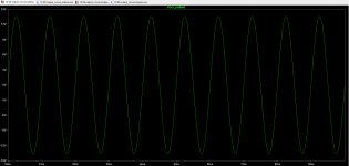
Yes, there is a major glitch near 23MHz and my 2 cents says it will oscillate. Since it is 3 decades outside the audio band it should be easy to slug-out. (Huh- dropped a default 1nFd cap in, it makes 79kHz smoooth as silk....)
I'm not worried you will turn this in because it uses techniques older than your teacher and he/she will wonder where you got it from.
Attachments
- Home
- Amplifiers
- Solid State
- Three stages amplifier college project help