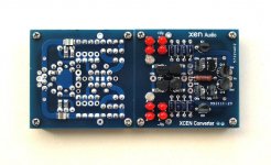
I got the PCBs today. Ohh man, are they tiny but very nice. I really have to learn SMD soldering better. It looks manageable though. Try to make it work over the weekend.
I am now building the XCEN. I have all components in house.
The soldering of the SMD resistors went smoother then i thought. Tomorrow i have a visitor and on friday i am away. Should be ready on the weekend though.
The soldering of the SMD resistors went smoother then i thought. Tomorrow i have a visitor and on friday i am away. Should be ready on the weekend though.
I got the PCBs today. Ohh man, are they tiny but very nice. I really have to learn SMD soldering better. It looks manageable though. Try to make it work over the weekend.
I use a clip to hold the chip in place for soldering, as well as very fine solder and a pointy tip on the iron. I keep a magnifier handy too.
You will not imagine how i do it : with my fingernails and without magnifier. I put a bit solder on one side, push the resistor down with my fingernail and solder. The other side is easy.
Gents, tweezers might help a bit!
No need for an especially pointy tip or fine solder either IMO. You want a reasonable size tip actually, if you are soldering anything with a large ground plane, your pointy tip will drop temp too quickly and have you leaving the soldering iron in place for too long.
A good light in the area helps a too.
<laughs> A few years ago I designed a complex central controller system for an Epson product, which included a number of innovative features including phase-sensitive decoding of motor state. When I brought one of the prototypes in for demonstration, primarily the clients were impressed that I had assembled it myself, as it was mostly surface-mount. They seemed much less impressed about the design, or that it worked 😀
For most parts, my technique is to apply solder to one pad, slide the part held by tweezers to the edge of that pad and reflow the solder as the part is positioned. Then it's a simple matter to solder the rest of the leads. If the lead pitch is really small sometimes you have to allow solder to bridge a few leads and then wick away the excess thereafter.
For most parts, my technique is to apply solder to one pad, slide the part held by tweezers to the edge of that pad and reflow the solder as the part is positioned. Then it's a simple matter to solder the rest of the leads. If the lead pitch is really small sometimes you have to allow solder to bridge a few leads and then wick away the excess thereafter.
Yes, tweezers help.
I have squeezed too hard with the tweezers and then the little microscopic chip goes flying never to be found again... 🙁
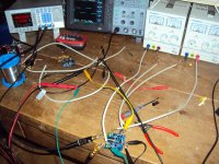
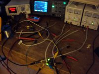
I made one board of the XCEN work. Common mode cancelation works well and both inputs reach over 2MHz without overshot. I have some offset that i will trim now. I then will build a second channel and listen. Technically the circuit is successful.
> Technically the circuit is successful.
Good to know. 🙂
And of course the PCB layout is error free. 😉
I shall be building myselfin 2~3 weeks (waiting for parts).
Then I shall post photos.
Patrick
Good to know. 🙂
And of course the PCB layout is error free. 😉
I shall be building myselfin 2~3 weeks (waiting for parts).
Then I shall post photos.
Patrick
It even has the slight overshot of the generator.
A stable square is often an advantage of a circuit without NFB.
No compensation, no nothing.
A stable square is often an advantage of a circuit without NFB.
No compensation, no nothing.
So test results of both prototypes as follows. It could not have gone more smoothly. 🙂
The circuit uses pre-calculated values of potential divider of the TL431s to account for the different Vgs of the Zetex MOSFETs.
Power supply was my lab supply, +/-24V, no on-board caps on the rails.
Supply cables are about 1m long.
On power up, DC offset was about 100mV, and no oscillations were observed with inputs shorted to Gnd.
The DC offset went down to about 30mV after 3 minutes.
Once it stabilised, the offset value was converted (by calculation) to trimming resistor values.
These were then soldered onto the PCB (1206 SMD resistors).
After trimming, DC offset at power up is now about 50mV, but dropping to less than 3mV in 5 minutes.
Within the next 20 minutes, it fluctuates between +/-5mV.
This corresponds to an offset current of 2.5µA at a total bis of 40mA for the entire circuit.
The TO92 JFETs and the E-line MOSFETs are at about 50°C at steady state, even though dissipation is only 100mW or so.
I am very confident that this can be improved by a factor of two by thermally coupling all devices to a heat spreader.
This we already planned from the start, but we wanted to test first before getting it manufactured, as it does add cost.
On top of the spreader (and the top of all FETs), will be mounted a CPU type heatsink of 45x45mm.
This will not only allow the different devices to track each other thermally.
It will also lower the overall temperature with the aid of the large heat sink.
And the thermal mass of the spreader and the sink will even out fluctuations with time.
As such, I personally do not think a servo is necessary, even though it can be added easily on an additional PCB underneath.
I can even live with 5mV as is.
The rest of the test is essentially same as Joachim, and same on both of my prototypes.
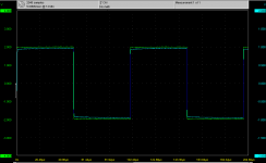
Bandwidth is -3dB, 2MHz. Perfect 10kHz square waves.
Gain is as predicted but can also be trimmed easily by adding a trim resistor.
Distortion is much lower than 90dB on 2Vrms, and beyond my measurement capability.
So that would have to wait till I get my hands on an AP again.
We already did a version 2 of the PCB where the left and right channels are mirror images.
And we also added electrolytic caps for the rails on board.
Once we get the thermal management tested, that would be it, as far as I am concerned.
QED. 🙂
Patrick
PS
On the DSO plot attached, green is input (functions generator 10KHz Sq), cyan is output.
Vin- was connected to Gnd in this case.
The circuit uses pre-calculated values of potential divider of the TL431s to account for the different Vgs of the Zetex MOSFETs.
Power supply was my lab supply, +/-24V, no on-board caps on the rails.
Supply cables are about 1m long.
On power up, DC offset was about 100mV, and no oscillations were observed with inputs shorted to Gnd.
The DC offset went down to about 30mV after 3 minutes.
Once it stabilised, the offset value was converted (by calculation) to trimming resistor values.
These were then soldered onto the PCB (1206 SMD resistors).
After trimming, DC offset at power up is now about 50mV, but dropping to less than 3mV in 5 minutes.
Within the next 20 minutes, it fluctuates between +/-5mV.
This corresponds to an offset current of 2.5µA at a total bis of 40mA for the entire circuit.
The TO92 JFETs and the E-line MOSFETs are at about 50°C at steady state, even though dissipation is only 100mW or so.
I am very confident that this can be improved by a factor of two by thermally coupling all devices to a heat spreader.
This we already planned from the start, but we wanted to test first before getting it manufactured, as it does add cost.
On top of the spreader (and the top of all FETs), will be mounted a CPU type heatsink of 45x45mm.
This will not only allow the different devices to track each other thermally.
It will also lower the overall temperature with the aid of the large heat sink.
And the thermal mass of the spreader and the sink will even out fluctuations with time.
As such, I personally do not think a servo is necessary, even though it can be added easily on an additional PCB underneath.
I can even live with 5mV as is.
The rest of the test is essentially same as Joachim, and same on both of my prototypes.
Bandwidth is -3dB, 2MHz. Perfect 10kHz square waves.
Gain is as predicted but can also be trimmed easily by adding a trim resistor.
Distortion is much lower than 90dB on 2Vrms, and beyond my measurement capability.
So that would have to wait till I get my hands on an AP again.
We already did a version 2 of the PCB where the left and right channels are mirror images.
And we also added electrolytic caps for the rails on board.
Once we get the thermal management tested, that would be it, as far as I am concerned.
QED. 🙂
Patrick
PS
On the DSO plot attached, green is input (functions generator 10KHz Sq), cyan is output.
Vin- was connected to Gnd in this case.
Attachments
Last edited:
Cool, i got the same result.
I will now wait for the new boards and then make a listening test.
I am quite confident though that this circuit is basically transparent and also can be used for other duty.
I will now wait for the new boards and then make a listening test.
I am quite confident though that this circuit is basically transparent and also can be used for other duty.
We already have n-versions on the drawing board.
MM Phono, HAGS (Head Amp Gain Stage), buffered filters, ....
🙂
P.
MM Phono, HAGS (Head Amp Gain Stage), buffered filters, ....
🙂
P.
- Home
- Source & Line
- Analog Line Level
- The XCEN -- Balanced to Single Ended Converter