Ouch, but like somebody else said, they might be ready at a buck apiece by the time this here contraption is... 😛Should be available any time now according to the original press releases.
I went to the sample page and they want a $35 "shipping and handling fee" for just a single piece; for 5pcs the fee is $147. 😱
So we may drop the zx driver.I have made some spice simulations of the zxgd3002 driver that i have post, and it has problems with dV/dT induced turn on because gate threshold voltage in this type of fet is very low.
I have made a new schema based in EPC demo boards, it is much better and the new parts are cheap.
Tomorrow i will test this.
Your discrete looks great, I don't mind going with discretes, especially if we can have greater control - for best performance. Also there are many complementary pairs in small packages (SC70 etc) around.
Eager to see the sim results...
E
Last edited:
Ok agreed let's leave them to professional audio thenThe Si8244 don´t have Output Sink Resistance low enough for preventing dV/dT induced turn on. and with this drive you can not chose Output Source Resistance, to slow down the turn on, and of course the eGaN FET only permits 6V of Vgs.
And, this type of drivers have problems with Pulse Width Distortion [...] you end-up with (5,6/1000)x100=0.56% error in open loop. This will result in poor noise and distortion performance of the amplifier.
This drivers are good for professional audio, but not for home Hi-Fi where minimum noise and distortion are required.

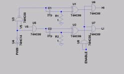
Meanwhile I have been toying with dead time control and going from PWM to HIN/LIN. The principle is easy enough, this sim gives DT from essentially 0 to around 1us when setting R1=R2 from 0 to 50KR. The prop. delays through the two arms should match.
Attachments
Ok agreed let's leave them to professional audio then
Pity, because the control of the dead time is very nice.🙁
Elevator,
What is the software that you use for designing PCB.
I'm very lazy in designing new parts 😱
If you use Eagle, i would be very grateful if you design this parts:
vishay Sia513, Si1029 and of course the eGaN FET.
You seem to be very fast in designing pcb 😀
Thanks.
What is the software that you use for designing PCB.
I'm very lazy in designing new parts 😱
If you use Eagle, i would be very grateful if you design this parts:
vishay Sia513, Si1029 and of course the eGaN FET.
You seem to be very fast in designing pcb 😀
Thanks.
Meanwhile I have been toying with dead time control and going from PWM to HIN/LIN. The principle is easy enough, this sim gives DT from essentially 0 to around 1us when setting R1=R2 from 0 to 50KR. The prop. delays through the two arms should match.
We only need like 5ns to 15ns.
One thing that would be nice, is a Dt control like the Si8244 use (only regulation in one resistor).
eagle pcb
Anybody else using eagle here?
E
I use protel 98 sp6. I have used eagle ~12 years ago for a short time, but am no longer proficient in it. Sorry.Elevator,
What is the software that you use for designing PCB.
I'm very lazy in designing new parts 😱
If you use Eagle, i would be very grateful if you design this parts:
vishay Sia513, Si1029 and of course the eGaN FET.
You seem to be very fast in designing pcb 😀
Thanks.
Anybody else using eagle here?
E
Sure, 1us is bad for distortion but good when you leave your beer on the heatsink and it's still cool after 10 minutes😀We only need like 5ns to 15ns.
One thing that would be nice, is a Dt control like the Si8244 use (only regulation in one resistor).
Seriously, 1us is way too much for the GaNs.
One resistor for both? I guess that would need two current mirrors?
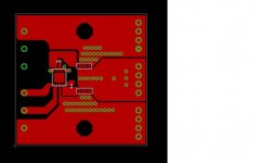
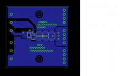
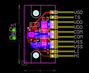
eGan driven by LM5113
E
Here's a quick stab at a module using the LM5113 as driver. Again, half-baked. Note the only components on the bottom are the EPC2010s. BTW I didn't find the LM5113 to be very layout-friendly. But maybe it's just me trying to avoid 0402 sized components.... You seem to be very fast in designing pcb 😀 Thanks.
E
Attachments
Last edited:
I use protel 98 sp6. I have used eagle ~12 years ago for a short time, but am no longer proficient in it. Sorry.
Anybody else using eagle here?
E
No problem Elevator 😎 . Thanks anyway.
I'm going 😴 .last night only sleep 2 hours, reading papers on the eGaN FET 😀
In this case I would flip the case, epoxy it down, and solder wires between pcb and fetYes, you are right, the thermal resistance of the bottom (Junction to Board) is very high, in the order of 16Cº /w , in the top (junction to case) is only 1.8Cº .
I abandon the idea of making the pcb with alu-core board, instead a double face pcb will be used with a heat sink or copper tongue attached to eGaN FET.
Last edited:
Its better to use larger C and R, so that you don't pich up as much noise and everything else, smaller R better... if possibleOk agreed let's leave them to professional audio then
Meanwhile I have been toying with dead time control and going from PWM to HIN/LIN. The principle is easy enough, this sim gives DT from essentially 0 to around 1us when setting R1=R2 from 0 to 50KR. The prop. delays through the two arms should match.
Compromise, compromise 😡 with more capacitance you create current spikes...Its better to use larger C and R, so that you don't pich up as much noise and everything else, smaller R better... if possible
15p is actually a lot, when you are in nanosecond territory. I am thinking of leaving a relatively high R as a stop-gap, but bringing both R-C nodes out to pins.
well, ok, will see then when we get there, what will be what...not saying that is must be like that
Be careful not to confuse depletion mode (Negative drive - piezo effect pulls structure apart) from enhancement mode (positive drive - piezo effect compresses structure).
Also, Tacky flux (Kester TSF-6592LV) with no solder paste or stencil works well. Be sure that all flux is cured before before applying power to avoid dendrite (tin whisker) growth.
Also, Tacky flux (Kester TSF-6592LV) with no solder paste or stencil works well. Be sure that all flux is cured before before applying power to avoid dendrite (tin whisker) growth.
Cool.I am already designing a board based in the LM5113.
Suggestions ?🙄
No snubbers? Or gate resistors?
Meanwhile I'm off on a slightly different direction, but here's my take on the LM5113 from a few days ago, schematic and layout (less auxiliary temp sensors). I didn't follow the NS layout guidelines exactly, because I did not want to use 0402 components.
Note the only components on the bottom side are the mosfets. This should ease the mechanical (assembly) problems. Also, I'd make sure that the last (2nd) reflow pass is for the bottom side, since the mosfets are soooo sensitive... Which BTW means that the top components will have to be glued.
Never a dull moment...
E
Attachments
Hmmm, you mean those mosfets actually get mechanically compressed and expanded? Idea:Be careful not to confuse depletion mode (Negative drive - piezo effect pulls structure apart) from enhancement mode (positive drive - piezo effect compresses structure).
 could I use them as loudspeakers? 😀
Curious about the diodes in series with the gate pull up resistors...Here's a quick stab at a module using the LM5113 as driver. Again, half-baked. Note the only components on the bottom are the EPC2010s. BTW I didn't find the LM5113 to be very layout-friendly. But maybe it's just me trying to avoid 0402 sized components.
E
Also from the layout I can't tell if the substrate pin (small pin next to gate) is connected to source of not. This is vital for operation as we found out.
Curious about the diodes in series with the gate pull up resistors...
Also from the layout I can't tell if the substrate pin (small pin next to gate) is connected to source of not. This is vital for operation as we found out.
Thanks EPCguy,
the diodes are a desperate measure. Somebody here remarked that 5V on the gate would kill the mosfets instantly, but OTOH the LM5113 wants at least 4.5V as Vdd. With Vdd=4.5V minus the diode drop, the mosfets would hopefully only go into a coma 😉
Noted re the substrate connection.
I also found that the LM5113 already pulls down the two inputs (HI and LI) so the two resistors are not needed.
E
- Status
- Not open for further replies.
- Home
- Amplifiers
- Class D
- The Uber eGaN Half-Bridge Module