I do not see a significant difference. Look at the crossings at +20V and -20V. The fall time looks to be about .7us and the rise time is about .8us.Interesting that the rise and fall behavior are different. Its like the brakes are on for the rise but the fall is a fall off a cliff until you get close to the bottom then the brakes engage. There are amusement park rides that behave that way.
The next tests are an attempt to better understand how the opto bias circuit behaves to a 100Hz, 50W into 8R signal burst having a 1/10 sec duration every 10 seconds. The SIT3X was adjusted for PFET M1 acting as much as possible as a current source.
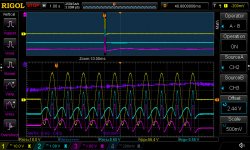
The trace colors are:
The interesting behavior is when the J1 SIT is maximally conducting (positive peaks of yellow trace) both J1bias and M1bias have some positive "blips". The purple trace is the difference J1bias-M1bias which increases by about 300mV during the signal burst, indicating that the bias current is increased by the burst. This agrees fairly well with simulations that I will post later.
The trace colors are:
- Yellow: Output (negative H1)
- Cyan: J1bias
- Magenta: M1 bias
- Purple: J1bias-M1bias
The interesting behavior is when the J1 SIT is maximally conducting (positive peaks of yellow trace) both J1bias and M1bias have some positive "blips". The purple trace is the difference J1bias-M1bias which increases by about 300mV during the signal burst, indicating that the bias current is increased by the burst. This agrees fairly well with simulations that I will post later.
Attachments
try 5 or 10sec burst
hardly relevant to real life situation, but handy to know how it will behave with modern rave (read- sustained DC) music
and do the same with 10KHz, maybe on smaller swing level
hardly relevant to real life situation, but handy to know how it will behave with modern rave (read- sustained DC) music
and do the same with 10KHz, maybe on smaller swing level
How many times a day do I get to carry this 50# beast up and down stairs between my listening area and my shop? I need to install a dumbwaiter. 🙁 Yes ZM, you are correct that a longer duration burst could be more informative.
Last edited:
there is just one solution for that - make listening and working area - the same
or make sissier amps, easy to carry around 🙂
there is also luckily one enormous benefit there - once when you declare that living room is strictly her (She, The Boss) domain, you'll be allowed to put amps and speakers of whatever size you wish
declaration is what counts 🙂
now seriously - see Pa's example - he didn't change neither speakers nor amps in living room for , what - a decade?
while in working music room, trolleys are sorta normal tool
(not that I'm telling here anything you didn't knew , already)
I actually have a relatively unused 18' x 25' room that could be made into combination shop and listening room. It would require significant sound conditioning since that floor is tile, and a 25' wall is mostly windows and sliding glass doors. I have considered this several times.
...I definitely like the SIT3X adjusted at the single-ended source-follower setting, where the M1 PFET is acting as a current source...
Have you listened with P6 set to minimum and R11 shorted?
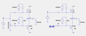
That setting, where the A parameter = 0, would have extreme Schade feedback, equivalent to connecting the gate of M1 to ground thru a capacitor as shown in schematic #3 of post #134 The SIT-3X Amplifier. This would cause rhe AC current through M1 to be a huge multiple of the AC current through J1 and of the same phase.
I have listened to the amplifier with values if A (and X) below the point where M1 is acting as a current source, as described in post #247. As the value goes lower, H2 increases and the class-A power level decreases further.
I have listened to the amplifier with values if A (and X) below the point where M1 is acting as a current source, as described in post #247. As the value goes lower, H2 increases and the class-A power level decreases further.
Oops, I missed the effect of connecting C4 to ground with The CCS being a P device, now I follow 'A < A_M1ccs push/push SIT signature magnified', thank you for clearing that up 🙂
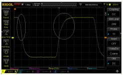
Very well behaved square wave response, is somewhat over damped. Basic low pass filter.
I'm trying to figure what size chassis and heatsinks will be needed to handle the power dissipation. I usually prefer a single chassis, but this may require monoblocks.
I'm trying to figure what size chassis and heatsinks will be needed to handle the power dissipation. I usually prefer a single chassis, but this may require monoblocks.
I measured the -3dB frequency to be at 420kHz with no C4FE input capacitor. With a 330pF capacitor the -3dB frequency is 89kHz.Very well behaved square wave response, is somewhat over damped. Basic low pass filter.
I'm trying to figure what size chassis and heatsinks will be needed to handle the power dissipation. I usually prefer a single chassis, but this may require monoblocks.
Monoblocks would solve the heatsink issue and might solve some ground loop issues I encountered due to my power supply layout.
In future posts I will discuss a possible successor design that runs at a lower voltage and could have a power dissipation low enough for the diyAudio Store Deluxe 5U Aluminum chassis. In that case, I would consider a single board FE design having grounding characteristics similar to the XA25 FE board.
I looked further at what would happen with A=0 as you suggested trying. In that situation, the combination of M1, C4, and R13 will act as a capacitance multiplier.
 Similar to a shunt reg...
I do not see a significant difference. Look at the crossings at +20V and -20V. The fall time looks to be about .7us and the rise time is about .8us.
Here is where I am talking about. Its like its overdamped approaching the flat top and underdamped coming off of the flat top.
I would saturate a sine wave and sweep frequency to investigate.
Its just curiosity.
Attachments
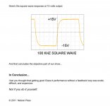
That curve is pretty typical square wave response and is roughly what you see from an 1st order low-pass RC filter. Here is page 13 of the Nelson's BA3 article: http://www.firstwatt.com/pdf/art_ba_3.pdf
Attachments
While doing bench testing today of the SIT3X to better understand the opto bias circuit behavior I managed to destroy a zener and filter cap. in the capacitance multiplier of one of the channels. I have seen the problem before when power the amplifier off and then back on after only 10 or 20 seconds, mainly blowing AC power fuses. There are likely multiple factors involved:
A major complication for the SIT/PFET source follower is that the gate voltage of the PFET needs to be more positive than that of the SIT. In order to reduce the bias current, the PFET gate voltage must be increased relative to the SIT. I still do not know the power off/on timing that creates the over current problem.
- The current surge limiters on the primary side of the power transforms are still hot and therefore their resistance is low.
- One or more capacitor in the bias circuit and perhaps elsewhere has only partially discharges and when power is restored, bias FET gate voltages are cause a bad current spike.
A major complication for the SIT/PFET source follower is that the gate voltage of the PFET needs to be more positive than that of the SIT. In order to reduce the bias current, the PFET gate voltage must be increased relative to the SIT. I still do not know the power off/on timing that creates the over current problem.
I think I found the problem I reported about blowing fuses and smoking components when the SIT3X was powered off and back on again too quickly (2sec-5sec). The capacitance multiplier 220uF capacitor C71 discharges very slowlt when the power is turned off, but the source and drain of the IRFP240 NFET M71 rapidly fall towards zero volts, thus Vgs is limited by the zener diode D71 to around 9.1V, which is very high. When power is restored, NFET M71 conducts with a very high current, recharging the 3.3mF capacitor C72 at around 1.5A for several seconds. This surge current is apparently enough to damage the capacitor.
The solution is to add a 1N4148 diode across R71 with its cathode connected to VR+. When the amplifier is powered off, this diode conducts and discharges C71.
The solution is to add a 1N4148 diode across R71 with its cathode connected to VR+. When the amplifier is powered off, this diode conducts and discharges C71.
Attachments
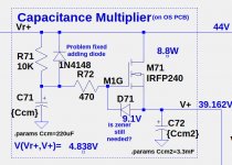
Yes, adding the 1N4148 diode makes sense. You have re-discovered the reason why that component commonly appears in the circuit for cap multipliers. It is also common to have another 1N4148 or even a 1N4003 from Source to Drain across the Mosfet to discharge the bulk capacitance after power-off.
Looking around at cap. multiplier circuits I never found one that included that diode. 🙄
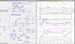
Here are some interesting waveforms from simulation. I do not believe that exact details, but the overall behavior looks correct.
The top waveform shows the relatively slow ramp up of the Vr+ voltage from the power supply when doing a cold start and the big inrush current limiters are still cold. Then after 20 secs the power is turned off, and after 2 secs back on. The negative rail behaves in the same manner with opposite polarity.
The other waveforms should be self explanatory, using device numbers and node labels from the schematic. The waveforms for V(M1G,V+) and I(C72) were the important ones to control. The 2nd turn-on current pulse thru C72 is now limited to only +34mA and .8W as opposed to about +1.4A and 30W.
Attachments
- Home
- Amplifiers
- Pass Labs
- The SIT-3X Amplifier