Many people use the current low voltage version for DAC with 5 V p.s. 250 mA shouldn't be a big problem: set CCS for 300 mA or more.
Disco's has been designed for <4V to overcome the minimum mosfet Vgs.
Disco's has been designed for <4V to overcome the minimum mosfet Vgs.
Use RG58 on all your shunts for sense wiring. Use as thick main ''force'' wiring as you like. Remember that the sense nodes are voltage nodes, don't worry about gauge. Their mission is to skip the voltage drop on the current carrying force wires and ''see'' the remote nodes directly. I believe that you will see less stuff on your scope in difficult termination situations if you shield your sense wiring. If you need extra thin and flexible enough, see about Belden (RG style) 179DT also, which I like for signal too BTW.
The Belden RG 179DT is a very good cable coaxial with 75 ohms impedance for digital SPDIF connexions too😉
The clear brown that I used in mine Simplistic Phono RIAA is a Huber-Shuner RG179 all teflon dielectric for the conductor & the shield, is a multistranded copper silver plated & also is a 75 ohms impendace, is extra thin 2mm but isn't flexible due to the teflon.
Can I use it for remote sensing? os is better to buy a RG58?
Both the noted TO-247 and TO-220 Mosfets can work on all schematics. Both types tested. 2N5457, BF245A for Q6 exchangeable. 2SK170 Q6 for the lower voltage range symmetric also. Up to 10uF MKT or MKP for C2. 47uF if with chemical cap. Output RC Zobel values are standard. Film cap there.
Some qestion to the low voltage 1.2 shunt
1. Q9 jfet should be from GR group ? ( it's not so easy to find 2n5459 with Idss>10mA)
2. What was the reason to use short gate Jfet as Q5 ??
1. Works with BL around 8mA. The 220R brings it far down. Its the low pinch off and noise that is of interest, current we tweak. If with GR, the 220R value should be revised lower. 5-6mA or more 2N5459 is enough in this occasion for cascode's top.
2. Many times has been written in the thread that only very low pinch off Jfets can work under just Vbe (0.6-0.7V) provided for Q5's position.
2. Many times has been written in the thread that only very low pinch off Jfets can work under just Vbe (0.6-0.7V) provided for Q5's position.
1. Works with BL around 8mA. The 220R brings it far down. Its the low pinch off and noise that is of interest, current we tweak. If with GR, the 220R value should be revised lower. 5-6mA or more 2N5459 is enough in this occasion for cascode's top.
2. Many times has been written in the thread that only very low pinch off Jfets can work under just Vbe (0.6-0.7V) provided for Q5's position.
So in case some Rs on the bottom cascode jfet is used , the rule of thumb is
Idss of the top casocode jfet > Id of the bottom jfet , where Id is settled by the value of the Rs ??
I'm little confused , because I was thinking the right rule is Idss of the top jfet always > Idss of the bottom cascode jfet.
I have to read once again Borbely articals and Siliconix AN103
Last edited:
It was confusing me too, because they don't discuss what happens if we degenerate the Idss. But I saw it works like this for real.
if a pair of cascoded jFETs are to be used.
Walt Jung says the voltage across the lower jFET should be at least twice the pinch off voltage.
This rule demands a low pinch off voltage for the lower jFET and also requires high transconductance.
A similar rule applies to the cascoding jFET. It too needs to see at least twice it's pinch off voltage to effectively cascode the inner/lower FET.
This cascoding FET must have a Vgs that is >2*Vpinch and this demands a highish Idss and a low transconductance.
I have found that
using BF244 or BF245 for the cascode and LSK170 for the lower jFET that
select a K170 with an Idss about 1mA to 1.4mA more than the required Id current and then the upper jFET needs approximately double this for it's Idss.
I don't know if this rule applies to other types.
eg. Id of the lower jFET is 3mA, then use a 4 to 4.4mA Idss 170 and add a 9mA 244 around it as the cascode.
The question is if we degenerate the inner jfet's idss to our needs, i.e lower than upper's, is it still the same condition? In practice it works as I saw. I don't know if perfect though. It comes very handy for using parts from our drawer. We may have the needed pinch offs but the lower jfet can be happier than OK for idss VS its upper in hand without using a resistor to drop.
I've made this layout for a + voltage v1.2 and was hoping that folks might take a look and give me feedback. I made it so that I could use a zener or resistor to set the voltage and with two pin out versions of Q2. All thoughts would be appreciated.
Thanks
Ken
Thanks
Ken
Attachments
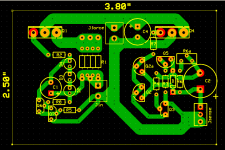
It doesen't look as a real v1.2..... I mean the lastest with film caps only.
Anyway, at 1st glace, R2 is too far from mosfet gate and C4 too close to hot component.
Also track to R7 seems to be too long due to the dual Tr.
My 2C
Anyway, at 1st glace, R2 is too far from mosfet gate and C4 too close to hot component.
Also track to R7 seems to be too long due to the dual Tr.
My 2C
The question is if we degenerate the inner jfet's idss to our needs, i.e lower than upper's, is it still the same condition? In practice it works as I saw. I don't know if perfect though. It comes very handy for using parts from our drawer. We may have the needed pinch offs but the lower jfet can be happier than OK for idss VS its upper in hand without using a resistor to drop.[/QUOTE
According to the Borbely , the top cascode jfet should be choosen from those , which have Vgs level >2V ( messured with the Id level= as the Id of the bottom cascode jfet , where the Id of the bottom cascode jfet is Rs depended
So in our case with Rs =220r,Id 1(bottom jfet) = 0,7mA
the top cascode jfet(2N5459) should have Vgs level (messured with the the Id = 0,7mA > 2V
It gives more Id with 8mA BL and 220R, around 1mA in practice, by measurement. But this will depend on each 2SK170's individual pinch off little tolerance 0.45-0.55V minus. From 2N5459 I get 6mA easily from most. Its pinch off can be 3-5V minus. Well sorted I guess?
P.S. Is it just >-2V or just >2X bottom fet's -Vp?
P.S. Is it just >-2V or just >2X bottom fet's -Vp?
It doesen't look as a real v1.2..... I mean the lastest with film caps only.
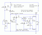
There are 2 ways to sort out V1.2's Vref and bypass. One that I recommend on best sonic grounds is to use the trimmer on jfet's source and use a high enough resistor decoupled with up to 10uF film, and a Zobel RC with filmcap on the output. Exactly as on page 190 ccts. Now if someone wants less drift than until a degenerated idss settles on a larger resistor, also needs be more secure about load interactions if can not have a scope to see, or not to go tuning the load's local bypassing, then the jfet can be run full idss, just g&s to ground, delete the 1k trimmer, and a 4k7 trimmer can be used instead of the 27k Rref. 220uF across 4k7 trimmer. Also a 47uf lytic instead of the Zobel. Now you lose gain progressively and the stability margin gains 25 degrees more. 80 deg in total. It gives a more typical tonal feel, bit more robust, less airy, less ''SE style''. Zo curve and value remains the same. The 1.2 reg is conceived as much simple & steady as possible with very common parts, but with quality beyond V1.0. Its TPC compensated and uses more but not very strong gain. So to keep noise at bay. That way films do work well enough. But if lytics in larger values are needed to swamp peculiar load interactions, of course it will play best with lytics. In general it will give a true resolution gain over 1.0 in any guise. You should hear it. Use best quality caps you can. An example with lytics is attached. Q1 can be IRF9610 and Q4 IRF9540 if you want TO-220. Polar caps must be reversed if applied to the negative schematic of page 190, goes without saying.
Attachments
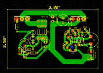
I've made this layout for a + voltage v1.2 and was hoping that folks might take a look and give me feedback. I made it so that I could use a zener or resistor to set the voltage and with two pin out versions of Q2. All thoughts would be appreciated.
Thanks
Ken
Hello Ken,
Maybe this is V1.0 45V like Merlin's?
Hello Ken,
Maybe this is V1.0 45V like Merlin's?
Yes, it's for approx 45v.
Ken
Anyway, at 1st glace, R2 is too far from mosfet gate and C4 too close to hot component.
Also track to R7 seems to be too long due to the dual Tr.
My 2C
Is this better?
Ken
Attachments
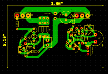
Looks neat to me, although I am as good in PCB evaluation as a Kick Boxer in fine arts.😀 I think you are closing sense- locally at the reg with force main ground? Wrong. Should be meeting only through cables at the load.
Looks neat to me, although I am as good in PCB evaluation as a Kick Boxer in fine arts.😀 I think you are closing sense- locally at the reg with force main ground? Wrong. Should be meeting only through cables at the load.
Salas,
Thanks, that make good sense 😉
Ken
Attachments
- Status
- Not open for further replies.
- Home
- Amplifiers
- Power Supplies
- The simplistic Salas low voltage shunt regulator