In the thread "DEF Amp",post #399, Nelson Pass explains how the Vgs differences alter the bias current.Thank you so much wwwtttwww!
Is it possible to post the .asc file? For the degeneration resistors, how many watts should these be rated for (ie, how much power goes through them)?
Is there any rough guidance on how much resistance to apply for a given difference between Vgs of SIT vs mosfet. For example in your case if you had a 1.2V difference and you applied (for example) 0.8R of degeneration ...
I'm oblivious to the math required to calculate this and I'm open to experimentation but would like to know that I have adequately rated resistors.
Thanks!
Stephen
Thanks wwwtttwww for the sim and thanks Claudio52 for the pointer to the DEF thread! Great work there as well Claudio52.
I pulled down Model info for the UJ3N120065K3S from United and modified wwwtttwww's model and it looks promising.
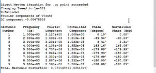
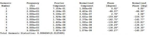
It's very nice and clean H2 (THD 0.0081% ) but it appears to be positive phase. Does anyone know offhand if the autoformer gain stage is inverting?
I'll report back if I make any progress but thanks for all the help getting me to this point.
Cheers!
Stephen
I pulled down Model info for the UJ3N120065K3S from United and modified wwwtttwww's model and it looks promising.
It's very nice and clean H2 (THD 0.0081% ) but it appears to be positive phase. Does anyone know offhand if the autoformer gain stage is inverting?
I'll report back if I make any progress but thanks for all the help getting me to this point.
Cheers!
Stephen
Attachments
Offset by +/-5% supply voltage variation
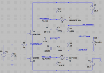
I used two SMPS for the simplest DEFiSIT with 2SK182ES. If the traditional linear PW is used, the fluctuation of power line will have significant effect on the amp offset, see 3 simulated pictures attached.
Left with nominal +/-24VDC, the offset is below 1mv.
Middle with +5% voltage, the offset -170mV , and Right with -5% voltage the offset +170mV.
Attachments
Last edited:
Add a Zenor
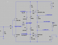
There is another simple way is worth to explore: just simply add a zener on the tail of R3 . The break voltage of the zener can be estimated as follow:
at 24VDC, adjust R4 to zero the offset, record Vg_Sit -4.41V, Vg_Mosfet -5.54V, the break voltage of zener should approximately 4.41+5.54=9.95V. Take the closest nominal 10V zener, R3 and R4 are well balanced.(See the attached pictures). The PW voltage with +/-5% fluctuations, the offset is +/-65mV, very acceptable.
Attachments
Last edited:
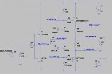
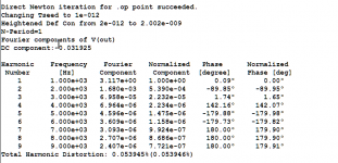
I use .tran 0 10ms 0 10n to sim. And got them.
2nd with -90. Very low thd+n.
Iq little bit too large.
2nd with -90. Very low thd+n.
Iq little bit too large.
Attachments
Last edited:
about 2A Iq
Attachments
-
 2021-06-22 21_56_25-SPICE Error Log_ C__Users_mxiao_Desktop_Pass Lab F5 Turbo v1_LTSpice_DEFiSIT.png26.1 KB · Views: 112
 -
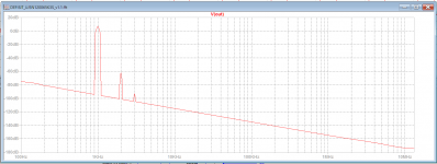
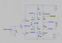
![2021-06-22 21_56_00-LTspice XVII - DEFiSIT_UJ3N120065K3S_v1.1[1].fft.png](/community/data/attachments/875/875832-fcc41838d639739e893d3f80b161370d.jpg?hash=_MQYONY5c5) 2021-06-22 21_56_00-LTspice XVII - DEFiSIT_UJ3N120065K3S_v1.1[1].fft.png31.3 KB · Views: 148
2021-06-22 21_56_00-LTspice XVII - DEFiSIT_UJ3N120065K3S_v1.1[1].fft.png31.3 KB · Views: 148 -
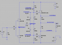
![2021-06-22 21_55_09-LTspice XVII - [DEFiSIT_UJ3N120065K3S_v1.1.asc].png](/community/data/attachments/875/875824-16676983b98b1b7a33e898b37c47ca4f.jpg?hash=Fmdpg7mLG3) 2021-06-22 21_55_09-LTspice XVII - [DEFiSIT_UJ3N120065K3S_v1.1.asc].png24.4 KB · Views: 151
2021-06-22 21_55_09-LTspice XVII - [DEFiSIT_UJ3N120065K3S_v1.1.asc].png24.4 KB · Views: 151
Next thing I need to figure out is how to generate FFT from LTSpice 🙂
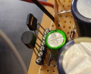
I have built up a protoboard and should be able to use this to test a variety of devices (hopefully). I'm using Wago quick release connectors on the output source connections so I can try paralleling different resistor values.
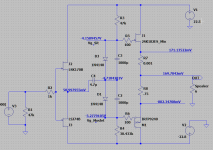
I see in the last sim from wwwtttwww that he has chosen to degenerate the P-channel mosfet to level match it (+1.7V) and as a result gets quite a high Iq around 2A which is roughly in line with what I was seeing in my measurements.
I have made some small changes in my proto - I didn't have any 4.7u film caps so I am using a bipolar electrolytic 10u Nichicon as it's nice and small and I am only interested in device selection at this point, not so much on the sound quality. The gain is too low to really try and judge it as well IMO.
I followed wwwtttwww's example for DC offset and am using a 15K in series with a parallel 50K + 200K pot which gives me a nice controllable adjustment range between 15K and 55K. I used degeneration on the N-DEF side instead of the P and according to the sim, if I use 0.05R degeneration, I can bring down the Vgs by estimated 658mV which is perfect 🙂. My questions if anyone can help - is as to how much power will be going through the degeneration resistors. I plan on using (2) 0.1R 3W resistors in parallel here and hope that it's sufficient but I also added 0.1R resistors between the power rails and the drains on the output devices as a convenient way to measure current draw. Is a single 3W resistor going to be ok here? I've seen and used 0.1R 3W resistors on power rails in other amps and they are ok so hoping that this will be the case here as well.
Last question I have is on whether or not I should be concerned for the front end JFETS as they are seeing 60mV but I don't know what the current going through them will be. Vgs through the gates of the output should be around 5.8V.
Any comments or words of warning before I attempt to power this up?
Thanks again to wwwtttwww for the encouragement to get me this far
Cheers,
Stephen
I have built up a protoboard and should be able to use this to test a variety of devices (hopefully). I'm using Wago quick release connectors on the output source connections so I can try paralleling different resistor values.
I see in the last sim from wwwtttwww that he has chosen to degenerate the P-channel mosfet to level match it (+1.7V) and as a result gets quite a high Iq around 2A which is roughly in line with what I was seeing in my measurements.
I have made some small changes in my proto - I didn't have any 4.7u film caps so I am using a bipolar electrolytic 10u Nichicon as it's nice and small and I am only interested in device selection at this point, not so much on the sound quality. The gain is too low to really try and judge it as well IMO.
I followed wwwtttwww's example for DC offset and am using a 15K in series with a parallel 50K + 200K pot which gives me a nice controllable adjustment range between 15K and 55K. I used degeneration on the N-DEF side instead of the P and according to the sim, if I use 0.05R degeneration, I can bring down the Vgs by estimated 658mV which is perfect 🙂. My questions if anyone can help - is as to how much power will be going through the degeneration resistors. I plan on using (2) 0.1R 3W resistors in parallel here and hope that it's sufficient but I also added 0.1R resistors between the power rails and the drains on the output devices as a convenient way to measure current draw. Is a single 3W resistor going to be ok here? I've seen and used 0.1R 3W resistors on power rails in other amps and they are ok so hoping that this will be the case here as well.
Last question I have is on whether or not I should be concerned for the front end JFETS as they are seeing 60mV but I don't know what the current going through them will be. Vgs through the gates of the output should be around 5.8V.
Any comments or words of warning before I attempt to power this up?
Thanks again to wwwtttwww for the encouragement to get me this far
Cheers,
Stephen
Attachments
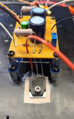
Picture of how I am connecting the output through Wago connectors for easy, flexible degeneration. In the previous post, you can see I just soldered wire to the source pins on the mos/sic-fets. The other end of the wire just goes to a Wago connector and since I am not degeneration the P-channel in this case, I didn't need the extra connector with jumper, I simply connect it directly to the output (connector).
On another note, super helpful member Dennis H pointed out the possibility of using the currently available FQA9P25 instead of the obsolete FQA12P20C and they are pretty closely interchangable. The sample FQA9P25 I tested in the harness measured 5.45V Vgs which is quite close to the average I was seeing for the obsolete devices. Once I verify that this is not too much of a gap (0.7V difference in Vgs), I will try it with FQA9P25 instead and the goal is to find currently available devices to make a DEF amp with. The icing on the cake will be to apply Schade feedback for some extra sweetness 🙂
Front end options seem to be multiplying like rabbits.
The other thing I noticed when building this was that there is only 2 ground connections - on the input and on the output, so if one were to do a single rail version it would be the easiest thing to just decouple input and output with caps and if one were to be completely unoriginal, you could even do an inverted single rail build 🙂
Cheers
Attachments

Next thing I need to figure out is how to generate FFT from LTSpice 🙂
Here is how I do it:
Attachments
Is it my imagination or is it not a good idea to slowly roll in the power with a variac with this one?
I have the board connected through a standard +/-24V linear supply (not using bench supplies) and the variac starts to buzz a bit and offset starts off crazy high (-4.5V) but current draw and offset seem to start to settle but I'm afraid of the transformer buzzing and back out before I get to 50%.
I don't have a dim bulb tester as I normally use the 4V fuses (mosfets and jfets) 🙂
Do I just set the variac to 100% and hit the switch from behind safety glass?
Nothing seems to have melted so far ...
Spoke too soon
Put meters on both rails for Iq and things were looking good when all of a sudden a sizzle and then a 'POP' sound ...
jfets were approx 6.5mA Idss ... should they be higher? Is the Vgs of these devices too high?
The headless jfet is the K170
Put meters on both rails for Iq and things were looking good when all of a sudden a sizzle and then a 'POP' sound ...
jfets were approx 6.5mA Idss ... should they be higher? Is the Vgs of these devices too high?
The headless jfet is the K170
Attachments


Should have sent in the stunt doubles to begin with...
Why didn't I learn from Star Wars? We almost lost Padme but lucky it was only Christensen this time. Now if only we could get rid of JarJar
Why didn't I learn from Star Wars? We almost lost Padme but lucky it was only Christensen this time. Now if only we could get rid of JarJar
Attachments
Last edited:
You can add 10-22 ohms resistor on the buffer jfet S.
I did sim with your set up. in Post 27, the Iq is too high, over 3A.
In #28, I changed your schematics, deleted two bias diodes. Its Iq is little bit over 2A.
My lsk170B and lsj74B are from the store. Their Idss are about 11mA. I have been running the amp for few weeks without any issue.
I did sim with your set up. in Post 27, the Iq is too high, over 3A.
In #28, I changed your schematics, deleted two bias diodes. Its Iq is little bit over 2A.
My lsk170B and lsj74B are from the store. Their Idss are about 11mA. I have been running the amp for few weeks without any issue.
Last edited:

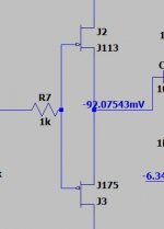
Have you measured Vgs, Id of Sic Jfet and Mosfet at24VDC?
What are they?
Even without the front buffer, you can check the Iq and offset of your power stage.
What are they?
Even without the front buffer, you can check the Iq and offset of your power stage.
I did measure them and posted that information in the DEF Amp Thread
Both measured @ 24V on heatsink
N-SIC UJ3N120065K3S
Id: 1.305A @ Vgs: -6.35V
P-MOS FQA12P20C
Id: 1.312A @ Vgs: -5.65V
Both measured @ 24V on heatsink
N-SIC UJ3N120065K3S
Id: 1.305A @ Vgs: -6.35V
P-MOS FQA12P20C
Id: 1.312A @ Vgs: -5.65V


OK.
If at 1.3A with 0.75 Rs, your Vg of PMOS should be -5.65-0.975=-6.625.
Vg_Sic-Vg_Pmos=-6.35-(-6.625)=0.275. If you add one diode between there will be 0.6V, this will push Vg_Sic higher and Vg_Pmos lower, Iq will be larger than 1.3A. You can start from one diode. Two may be too many.
If at 1.3A with 0.75 Rs, your Vg of PMOS should be -5.65-0.975=-6.625.
Vg_Sic-Vg_Pmos=-6.35-(-6.625)=0.275. If you add one diode between there will be 0.6V, this will push Vg_Sic higher and Vg_Pmos lower, Iq will be larger than 1.3A. You can start from one diode. Two may be too many.
- Home
- Amplifiers
- Pass Labs
- The simplest DEFiSIT with 2SK182ES