Compared to bipolar supply, a single supply DEF with output cap has better PSRR and provides additional safety layer for the speakers.

I removed the diodes and 1000u caps and checked the connections but I'm not sure if the 0.1R current reading resistors is causing me problems or if it's saving my neck because they are getting really hot even at very low rail voltages. I am slowly bringing it up with the variac and reading 600mV over 0.1R or 6A going through each rail. Rough math gives 3.6W so it's no wonder these are starting to smoke (3W rated) an hit over 120C (temperature) ...
I guess if the rail voltage is not high enough, the depletion mode device will be wide open but I don't understand why both rails are drawing so much current.
 😕😕😕
😕😕😕
I guess if the rail voltage is not high enough, the depletion mode device will be wide open but I don't understand why both rails are drawing so much current.
😕😕😕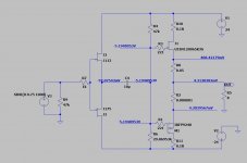
If you like zero or small degenerating, you have to have perfect matched NJet and PMos at Vds, Vgs and Iq condition.
For not ideal components, either R8 or R2 has to be much larger than you used.
Your Vgs of NJet at 1.3A is lower than Vgs of PMos. If using the schematics in#45, Iq is huge. It is not going to work.
For not ideal components, either R8 or R2 has to be much larger than you used.
Your Vgs of NJet at 1.3A is lower than Vgs of PMos. If using the schematics in#45, Iq is huge. It is not going to work.
Last edited:
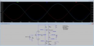
Went back to the drawing board and played around with the degeneration.
With 1.5R degeneration, it's possible to get the current draw down to 1.4A and it looks like it doesn't really matter which device gets the degeneration but you can decide to drive one side through greater current swing than the other depending on how you distribute the total degeneration resistance.
If one were to apply Schade feedback to one of the devices and distributed the degeneration to cause that side to have greater voltage swing, would that effectively increase that side's influence on the sound? (my crazy conspiracy theory).
Blew out the IEC fuse last night with the bad circuit (the one that was trying to draw 8A through each rail) so I'm taking a break from the soldering iron at least for now
Attachments
- Home
- Amplifiers
- Pass Labs
- The simplest DEFiSIT with 2SK182ES