OK. I am unable to model -6.2mA on both the + and - pins of the current generator in Tina. So, I just modeled this part of the schematic and set the generator to 7.8mA sine wave with a -6.2mA DC offset. Performance is very good but there's a DC offset of -1.55V on the output. I don't know if that's a big deal. Distortion, noise and bandwidth are all excellent. S/N is 140dB. I'm impressed. The NE5534 performs extremely well. Input noise is 13picoV/Hz^0.5. Gain is just right at about 50dB. Of course, I adjusted the feedback resistor to achieve that. It seems to be fine at low resistor values. The outputs are running at 23mA. I didn't spend much time optimizing it.
Hi Dirk
thanks for simulating the NE5534. I have to try TINA .
Can I just ask you to simulate the same circuit but without the buffers?
Just to see the differences.
I do not know if a constant current source is better. Hard to make one that drops only 0.65V, i wanted to use the existing constant current source of the buffer. Theoretically yes, the NE would see a higher impedance. On the other hand i build circuits like that ( with the resistor ) that worked respectable. A separate constant current source could of cause being made connected not to the output node but to the positive supply.
I think the resistor connected like you suggest will turn off the output npn transistor of the NE5534 , is this what you pretend ? the NE5534 will perform better with the npn transistor turn off ?
No, i wanted to turn off the PNPs. In fact the NE does not even have PNPs in the output but a very tricky substitute. I had a hard day , sorry. The buffer i use looks very similar but is in detail different from Dirks. Important is that the constant current is inserted from the positive supply whereas most circuits you can see on the web bias the opamps to the negative supply. That does not work with the NE.
That is interesting. I have to take a better look to the internal circuit of NE5534.
If you can post more information about this would be very helpful.
good night.
If you can post more information about this would be very helpful.
good night.
Here is some information on a headphone amp that uses that option. Unfortunately the website is not fully online so the circuit is not visible but there is enough to understand it.HeadWize: DIY Workshop > Headphones amp based on the ne5534
I can´t stop, here is the full monti. A phono stage based on the NE5534 i designed with all possible workarounds.
This last circuit is very clever. I think is a very good idea using the pin 5 as output.
the output pnp can not be turn off , it has a local feedback loop.
to increase quiescent current we need to turn off the npn, or bypassing by using the pin 5.
we can use the 220 ohms resistor that you suggest and use the pin 5 as output. what do you think.
Edit: when I say output pnp I meen lower npn.
Last edited:
Well, this is how far i went. To pimp up that old stablemate is fun though. I run out of design power for today.
You could put a ccs from the output of the op amp to the negative voltage rail to bias
the output into class A and use only the npn part of the op amp output.
the output into class A and use only the npn part of the op amp output.
 Gentlemen. Please use the Quote button with restraint.
Do not quote the entire post just above yours.
I have removed much of the over-quoting.
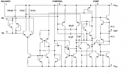
avro look to post 145. this opamp is a litle bit different. it uses 2 npn output transistors and the lower transistor can not be turn off . so in this case is better to connect the ccs to the +vcc and use only the lower npn transistor.
Hi Dirk
thanks for simulating the NE5534. I have to try TINA .
Can I just ask you to simulate the same circuit but without the buffers?
Just to see the differences.
I can tell you now that the NE5534 is not going to be able to drive the feedback loop. Minimum load allowed on that chip is 600 ohms.
There is no problem you can put a 150ohms as the feedback resistor the current that passes throw that resistance is the dac current out 7.8ma pp. the maximum current is 38ma.
But you don't need,to do a simulation it only make sense simulate the all circuit .
And one way or another , as Jcx has already told in post 52, the opamp models are not very good.
How is your IV project?
But you don't need,to do a simulation it only make sense simulate the all circuit .
And one way or another , as Jcx has already told in post 52, the opamp models are not very good.
How is your IV project?
- Status
- Not open for further replies.
- Home
- Source & Line
- Digital Source
- The pcm1794a datasheet I/V converter and how to improve it.