Luke,
Convert the internal dimensions, establish your full set of working (cut) dimensions from them & check the baffle width. A few mm or fraction of an inch difference of baffle width is insignificant.
Sorry Ed I missed your reply. Yes this approach makes sense. My biggest decision is whether I buy or build. Buy (used) and you have resale as well you can listen first. Build and its a lottery. I've been waffling about this for a year🙂
On post 1774 I see the last schematic but it is about 200W desing on plus and minus 70 volts dDC , did somebody downsise the amp to 100W or so on a 40-0-40 volts transformer ....or ... plus and minus 56 volts DC
I posted the 120w version on post 1808/9. This is with +/- 45v - 60v rails.
Your probably better of holding out a little longer and building this though.
http://www.diyaudio.com/forums/solid-state/192431-class-ab-amp-diyaudio.html
According to Os, its an improved version of the Mongrel series.
Your probably better of holding out a little longer and building this though.
http://www.diyaudio.com/forums/solid-state/192431-class-ab-amp-diyaudio.html
According to Os, its an improved version of the Mongrel series.
Audiofan: I did some downsizing.
I tried to reduce the gain somewhat since I needed less of it then originally designed for. With the AX-board the amp ran into some small oscillation with the TMC due to the reduced phasemargin. This was discussed a few pages ealier.
OS suggested in post 1794:
"You could increase the 2 input pair degeneration resistors to 180-220R and up the negative feed back resistor to 22K (gain of @ 25). This will bring you back to 370-400K unity gain crossover with >90 degrees margin. (stable again - below 2) "
I did this (and also some LT-spice simulations) but have not yet put back the TMC. What I can say is that with ordinary miller compensation it is really stable. Right now I am using a 38-0-38V transformer which is similar to your 40V. Need some more testing though before I can say I have finished it completely. I am using the "big" PB250 since I will use 4 Ohm speakers and want to share the current between more output transistors, but I guess the 120W version will be good as well.
Hi
What type of test equipment do you like to use for measuring performance ?
Maybe you could post some of your measured specifications.
It would be Fun and Useful to see some pictures of the mechanicals.
.
Did you have a chance to build a unit as specified in the documentation ?pellesand
I am trying to figure out what functional problems were caused by your redesign of the circuit. Oscillations, TMC and phase margin are serious concerns. Were there any improvements in the operation of the circuit with your changes ?"I tried to reduce the gain somewhat since I needed less of it then originally designed for. With the AX-board the amp ran into some small oscillation with the TMC due to the reduced phasemargin."
Could you please supply the LT simulation files that you used for your simulation to show the operation of the circuit. It is a serious concern if the amplifier does not work properly As Originally Designed or because of Minor component value changes."OS suggested in post 1794:"
"You could increase the 2 input pair degeneration resistors to 180-220R and up the negative feed back resistor to 22K (gain of @ 25). This will bring you back to 370-400K unity gain crossover with >90 degrees margin. (stable again - below 2) "
"I did this (and also some LT-spice simulations) but have not yet put back the TMC."
What type of test equipment do you like to use for measuring performance ?
Maybe you could post some of your measured specifications.
It would be Fun and Useful to see some pictures of the mechanicals.
.
ArtM;
What I did was that I reduced the gain to ~20. I do not have the schematics in front of me but I think the orignial gain was close to 40. This will lead to some changes in phase margin but I at this point I just hoped it would work, but i didn't. So I reduced the gain by 50% and that introduced some oscillation at some points. As OS said (post 1794) I reduced the gain to much, getting to low phase margin. By the changes he suggested the gain was still not as high as the original, but the amp stable. OS showed the simulations in post 1794. My own simulations was just repeating this and playing around with some resistor values. The model was posted in post 1797 (in the spice model mongrelmodels.txt is included, change that name to the name of the model file supplied in the zip) . After changing the values to the ones suggested by OS the amp behaves as it is supposed to. For the original values of the components I firmly believe the amp is very stable.
For the testing I used a waveform generator (HP33120A), Oscilloscope (Tektronix TDS3012). As loads I have used a 50W/4Ohm power resistor (It got very warm at high power..) as well as some speakers. I have also tested using a CD-player as source. I would like to measure distortion but I do not think I have access to any good enough equipment. Next step is to finish putting together all parts in the case and test with my better speakers. Then I will show some pictures
Changing the closed loop gain from 40Times (+32dB) to 20Times (+26dB) completely changes the way the feedback interacts with the amplifier, particularly the gain margin and phase margin.
If the 20kHz feedback was 17dB when gain was +32dB (for an open loop gain @ 20kHz of +47dB), then that 20kHz feedback must change to 23dB when the lower gain is asked for.
That change in HF feedback is absolutely critical to phase margin.
Compare the simulator predictions for the two gains you want to play with. I think when you ask the correct questions, the predictions answers will be quite illuminating.
LTC Spice examples
pellesand and AndrewT:
Thanks for your response. I will play around with the LoopGain and LoopGain2 examples in the LTC Spice Educational file to gain a Gut feeling for phase margins.
pellesand and AndrewT:
Thanks for your response. I will play around with the LoopGain and LoopGain2 examples in the LTC Spice Educational file to gain a Gut feeling for phase margins.
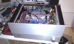
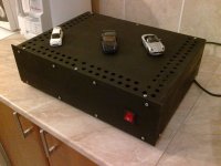
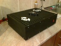
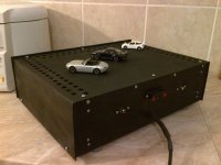
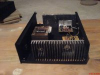
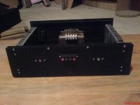
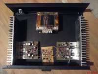
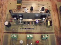
After building occasionally for the last half year I put the lid on to my AX-PB250 combo today.. It sound very nice and it does not loose grip of the speakers even at very high volume. Much better then my old arcam A75 in all respects, The old amp temporaily acts like a preamplier until I've finished the one I am building (below in image). I will get there some day....
For a while I had some hum problem, very weak but audible close to the speaker. By rearranging ground connections and cabling it became lower but did not disappear totally. It also got worse when connecting the pre-amp, indicative of a external ground loop. It turned out that the ground lift diodes, D1 and D2, both had blown on both boards. On one board one was shorted and the other one open. On the other both shorted. Must have happened during early testing where also some transistors blew. However, after replacing the diodes it is really silent
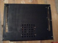
The board upside down in the back of the amp is a speaker DC protection and delay circuit. There was no space for it other then mountning it on the lid.
Thanks to OS and al others involved in this design.
/Pelle
For a while I had some hum problem, very weak but audible close to the speaker. By rearranging ground connections and cabling it became lower but did not disappear totally. It also got worse when connecting the pre-amp, indicative of a external ground loop. It turned out that the ground lift diodes, D1 and D2, both had blown on both boards. On one board one was shorted and the other one open. On the other both shorted. Must have happened during early testing where also some transistors blew. However, after replacing the diodes it is really silent
The board upside down in the back of the amp is a speaker DC protection and delay circuit. There was no space for it other then mountning it on the lid.
Thanks to OS and al others involved in this design.
/Pelle
Attachments
dear all mogrel reader,
i want pcb and details of power amplifier using transistor 2sk1058 and 2sj162.my email is khan.shahid251@gmail.com i want to construct on the of new year.thanks and gretings to all.your ever masood alvi
i want pcb and details of power amplifier using transistor 2sk1058 and 2sj162.my email is khan.shahid251@gmail.com i want to construct on the of new year.thanks and gretings to all.your ever masood alvi
The amp in this thread is not a mosfet design. Plenty of schematics around using the parts you mention. No free lunch - it's called *DIY* audio.
Finally the last page...
nikko (http://www.diyaudio.com/forums/solid-state/169590-mongrel-supersym-ii-129.html post #1287) has given me a pcb of SymAsym a few years ago,and told me that this would be logical next step. Recently i have re-done a SymAsym case and i am listening it right now. I have another case with 1kVA transformer with 2 x 35Vac,heatsinks and 4x20 000uF in PSU and some parts. I have asked nikko for files but he had some troubles with his computer,his hard-disc collapsed so i decided to search for a whole thread to find needed files. So i started with page one,have read a lot of things i don´t quite understand (i´m a beginer and practically just assembler,but anyway i cought some guidelines "how and why" ) and on page 181 post #1808/1809 found all i need-thanks to repeet!
OS did a great job here,he shared each step he did with the readers,fought out on his own with all opsticles that were before him and unselfishly shared numerouse files and experiences with all of us. THANK YOU SO MUCH OS!
One question for a start-i have two pairs of MJE21193/MJE21194,can i use them as output transistors? Also i have two pairs of 2SA1943/2SC5200,wich (if any) would be better replacement?
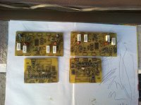
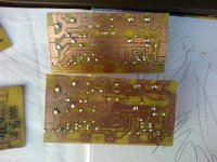
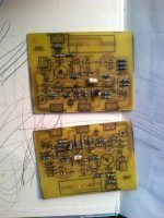
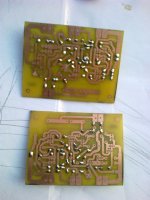
Here are some pictures of SymAsym,and hope soon there will be some pistures of a PB120N.
nikko (http://www.diyaudio.com/forums/solid-state/169590-mongrel-supersym-ii-129.html post #1287) has given me a pcb of SymAsym a few years ago,and told me that this would be logical next step. Recently i have re-done a SymAsym case and i am listening it right now. I have another case with 1kVA transformer with 2 x 35Vac,heatsinks and 4x20 000uF in PSU and some parts. I have asked nikko for files but he had some troubles with his computer,his hard-disc collapsed so i decided to search for a whole thread to find needed files. So i started with page one,have read a lot of things i don´t quite understand (i´m a beginer and practically just assembler,but anyway i cought some guidelines "how and why" ) and on page 181 post #1808/1809 found all i need-thanks to repeet!
OS did a great job here,he shared each step he did with the readers,fought out on his own with all opsticles that were before him and unselfishly shared numerouse files and experiences with all of us. THANK YOU SO MUCH OS!
One question for a start-i have two pairs of MJE21193/MJE21194,can i use them as output transistors? Also i have two pairs of 2SA1943/2SC5200,wich (if any) would be better replacement?
Here are some pictures of SymAsym,and hope soon there will be some pistures of a PB120N.
Attachments
Dear Borina,
2SC5200/A1943 are better than MJE21193/MJE21194 in matter of ft and beta linearity, by a large margin, wich, for me, are more important than few more watts of dissipation allowed by Motorolas.
Maybe another ones have a different opinion.
Regards,
Marcos
2SC5200/A1943 are better than MJE21193/MJE21194 in matter of ft and beta linearity, by a large margin, wich, for me, are more important than few more watts of dissipation allowed by Motorolas.
Maybe another ones have a different opinion.
Regards,
Marcos
Dear Borina,
2SC5200/A1943 are better than MJE21193/MJE21194 in matter of ft and beta linearity, by a large margin, wich, for me, are more important than few more watts of dissipation allowed by Motorolas.
Maybe another ones have a different opinion.
Regards,
Marcos
He he,my name is Aleksandar(that is how it is written in my language) ,the links under my posts are to FB-profile and FB-page wich are dedicated to boraomega´s designes (dr.Borivoje Jagodić) so that is how is the profile named "Borina Pred Pojačala" or in english- "Bora´s Pre Amplifiers". All the albums are sorted by specific designes.
Thank you for your answer 😉 i will post pictures as i do some progress...
I have a few questions about CX 1.3 VB-U
The emitors and collectors of Q3 and Q4 on layout have switched their places comparing to a schematics.
1;On schematics the emitter of Q3 goes to a collector of a Q1,and by layout the collector of Q3 goes to collector of a Q1.
2;On schematics the emitter of Q4 goes to a collector of a Q2,and by layout the collector of Q3 goes to collector ofa a Q2.
3; R8 exists on a layout and picture of finnished pcb but there is no R8 on a schematics.
4; Also,places of R16 and R17 are switched.
Could anybody please help me about this...
Attachments
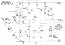
I have done that,and pinout of transistors are correct as they are on right down square of a schematic. Same thing is in VRT,so the pinout for him self is ok.First thing I would check is transistor numbers and pinout for these transistors.
The pinout on a pcb is not,and I think that the pins E and C should switch places.
The resistors R16 and R17 should switch places too,and judging about a text that says "12/15V zener optional for R17" the value of R17 should be 15kOhm because in series with 56kOhm and about 50Vdc supply the voltage on the base of Q3 and Q4 would be 12Vdc.
R8 is one thing more,i can´t find it on a schematic and it exists on layout and even on a picture of a finished pcb. I am a beginner in these things and my questions are maybe nonsense but i´d say this time i´m right...
Thanks for your interesting here! 🙂 (and sorry for my not so good english...)

- Home
- Amplifiers
- Solid State
- The MONGREL (supersym II)